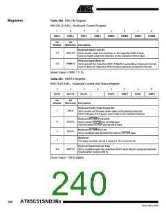
Registers
Table 255. LCDCON0 Register
LCDCON0 (1.96h) – LCD Control Register 0
7
6
5
4
3
2
1
0
BUINV
LCIFS
ADSUH1
ADSUH0
ACCW3
ACCW2
ACCW1
ACCW0
Bit
Bit
Number
Mnemonic Description
Busy Invert Active
7
BUINV
Set to check busy bits selected in LCDBUM as active low.
Clear to check busy bits selected in LCDBUM as active high.
Interface Select Bit
6
LCIFS
Set to select 6800 interface type.
Clear to select 8080 interface type.
Address Setup/Hold
5-4
ADSUH1:0
Address Setup and hold length in clock periods (from 1 to 4 clock periods).
Access Cycle Width
Access width in clock periods (from 1 to 16 clock periods).
In 8080 mode, corresponds to WR or RD low state.
In 6800 mode, corresponds to E high state.
3-0
ACCW3:0
Reset Value= 0000 0000b
Table 256. LCDCON1 Register
LCDCON1 (1.8Eh) – LCD Control Register 1
7
6
5
4
3
2
1
0
SLW1
SLW0
RSCMD
LCYCW
LCYCT
LCEN
LCRD
LCRS
Bit
Bit
Number
Mnemonic Description
Sleep Wait States
Busy check process enabled
Number of wait states between a read or write access and a busy check process
(from 1 to 4 clock periods).
7-6
SLW1:0
Busy check process disabled
Number of wait states between two read or write accesses (from 1 to 4 clock
periods).
RS Command/Status
Set to output high level on LA0/LRS pin during busy check process.
Clear to output low level on LA0/LRS pin during busy check process.
This value depends on the LCD controller.
5
4
RSCMD
LCYCW
Deassertion Cycle Width
Set to program E or RD/WR signals deassertion time to the number of clock set
in ACCW3:0 bits.
Clear to let E or RD/WR signals deassertion time to the number of clock set in
ADSUH1:0 + SLW1:0.
236
AT85C51SND3Bx
7632A–MP3–03/06

 ATMEL [ ATMEL ]