AT85C51SND3Bx
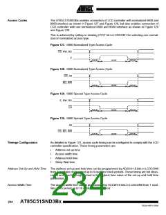
Sleep Wait Time
The sleep wait time is the time between two consecutive access cycle. It can be pro-
grammed by SLW1:0 bits in LCDCON1 from 1 oscillator clock period up to 4 oscillator
clock periods
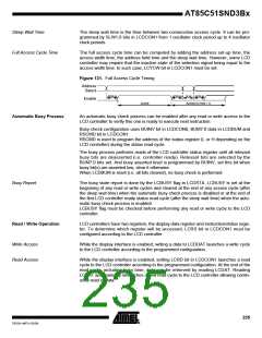
Full Access Cycle Time
The full access cycle time can be computed by adding the address set-up time, the
access width time, the address hold time and the sleep wait time. However, some LCD
controller may require that the inactive state of the selection signal being equal to the
access width time. In such case, LCYCW bit in LCDCON1 must be set.
Figure 131. Full Access Cycle Timing
Address
Select
ADSUH
ADSUH SLW ADSUH
ACCW (LCYCW = 1)
Enable
ACCW
Automatic Busy Process
An automatic busy check process can be enabled after any read or write access to the
LCD controller to verify this one is ready to execute next instruction.
Busy check configuration uses BUINV bit in LCDCON0, BUM7:0 data in LCDBUM and
RSCMD bit in LCDCON1.
RSCMD is used to program the address of the status register (L or H depending on the
LCD controller) during the status read cycle.
The busy process performs reads of the LCD controller status register until all relevant
busy bits are deasserted (i.e. controller ready). Relevant bits are selected by the
BUM7:0 bits set. And busy asserted level is programmed by BUINV, set this bit when
busy bit(s) are asserted low, clear it otherwise.
When LCDBUM is reset (i.e. all bits cleared), no busy check is performed.
Busy Report
The busy state report is done by the LCBUSY flag in LCDSTA. LCBUSY is set at the
beginning of any read or write cycles and cleared at the end of any access cycle (after
the sleep wait time) when the automatic busy check process is disabled or at the end of
the first LCD controller ready status read cycle (after the sleep wait time) when the auto-
matic busy check process is enabled.
LCBUSY flag must be checked before performing any read or write cycle to the LCD
controller.
Read / Write Operation
LCD controllers have two registers, the display data register and instruction/status regis-
ter. To determine which register will be accessed, LCRS bit in LCDCON1 must be
configured according to the LCD controller.
Write Access
Read Access
While the display interface is enabled, writing a data to LCDDAT launches a write cycle
to the LCD controller according to the programmed configuration.
While the display interface is enabled, setting LCRD bit in LCDCON1 launches a read
cycle to the LCD controller according to the programmed configuration. At the end of the
read cycle, including busy time, data can be retrieved by reading LCDAT. Reading
LCDAT automatically relaunches a new read cycle to the LCD controller allowing contin-
uous read of data.
235
7632A–MP3–03/06

 ATMEL [ ATMEL ]