AT85C51SND3Bx
Display Interface
The AT85C51SND3Bx implement a display interface allowing glueless direct interfacing
(thanks to its highly configurable capability) to almost all of the LCD controllers found in
either graphic or text LCD display.
These LCD controllers interface is from either 6800 or 8080 compatible type with some
variant in the implementation.
The display interfaces to the C51 core through the following special function registers:
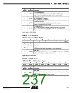
LCDCON0, LCDCON1, the LCD control registers (see Table 255 and Table 256); LCD-
STA, the LCD status register (see Table 257); LCDBUM, the LCD busy mask register
(see Table 258); and LCDDAT, the LCD data register (see Table 259).
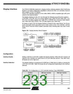
As shown in Figure 126, the Display Interface is divided in two major blocks: the Access
Cycle Generator which generates read or write cycles to the LCD controller, and the
Busy Check Processor which enables automatic busy checking after any read or write
cycles.
Figure 126. Display Interface Block Diagram
LCDCON1.1 LCDCON1.0 LCDCON1.7:6
OSC
LCRD
LCRS
SLW1:0
CLOCK
LCIFS
LWR/LRW
LRD/LDE
LA0/LRS
LCS
LCEN
LCDCON1.2
LCDCON0.6
LCDCON1.5
LCYCT
LCDCON1.3
Access Cycle
Generator
RSCMD
LD7:0
Busy Check
Processor
LCBUSY
LCDCSTA
LCYCW ADSUH1:0 ACCW3:0
LCDCON1.4 LCDCON0.5:4 LCDCON0.3:0
BU7:0
LCDBUM
BUINV
LCDCON0.7
Configuration
Interface Enable
Setting LCEN bit in LCDCON1 enables the display interface. When this bit is cleared, all
signals to the controller are switch back to I/O port alternate function. Thus after reset,
all signals are set to high level.
Interface Selection
The display interface is programmed in 6800 type or 8080 type by setting or clearing the
LCIFS bit LCDCON0. Table 254 shows the pin configuration depending on the interface
selected.
Table 254. Pin Configuration vs. LCD Controller Interface Type (6800/8080)
Pin Name
LWR/LRW
LRD/LDE
LA0/LRS
LCS
8080 Type Controller
6800 Type Controller
WR
RD
RW
E
A0
RS
CS
D7:0
CS
LD7:0
D7:0
233
7632A–MP3–03/06

 ATMEL [ ATMEL ]