AT8xC51SND2C
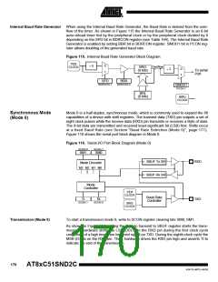
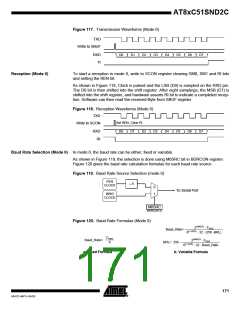
Figure 117. Transmission Waveforms (Mode 0)
TXD
Write to SBUF
RXD
TI
D0
D1
D2
D3
D4
D5
D6
D7
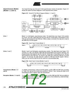
Reception (Mode 0)
To start a reception in mode 0, write to SCON register clearing SM0, SM1 and RI bits
and setting the REN bit.
As shown in Figure 118, Clock is pulsed and the LSB (D0) is sampled on the RXD pin.
The D0 bit is then shifted into the shift register. After eight samplings, the MSB (D7) is
shifted into the shift register, and hardware asserts RI bit to indicate a completed recep-
tion. Software can then read the received Byte from SBUF register.
Figure 118. Reception Waveforms (Mode 0)
TXD
Set REN, Clear RI
D0 D1 D2
Write to SCON
RXD
RI
D3
D4
D5
D6
D7
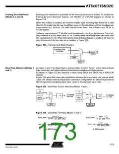
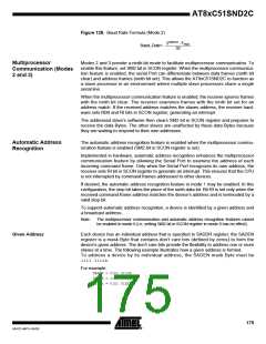
Baud Rate Selection (Mode 0) In mode 0, the baud rate can be either, fixed or variable.
As shown in Figure 119, the selection is done using M0SRC bit in BDRCON register.
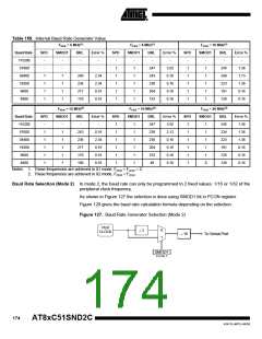
Figure 120 gives the baud rate calculation formulas for each baud rate source.
Figure 119. Baud Rate Source Selection (mode 0)
PER
CLOCK
÷ 6
0
To Serial Port
1
IBRG
CLOCK
M0SRC
BDRCON.0
Figure 120. Baud Rate Formulas (Mode 0)
2SMOD1 ⋅ FPER
Baud_Rate=
6(1-SPD) ⋅ 32 ⋅ (256 -BRL)
FPER
2SMOD1 ⋅ FPER
Baud_Rate=
6
BRL= 256 -
6(1-SPD) ⋅ 32 ⋅ Baud_Rate
a. Fixed Formula
b. Variable Formula
171
4341D–MP3–04/05

 ATMEL [ ATMEL ]