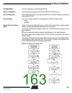
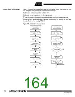
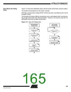
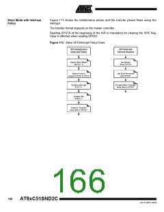
AT8xC51SND2C
Registers
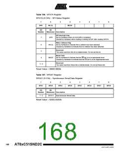
Table 155. SPCON Register
SPCON (S:C3h) – SPI Control Register
7
6
5
4
3
2
1
0
SPR2
SPEN
SSDIS
MSTR
CPOL
CPHA
SPR1
SPR0
Bit
Bit
Number
Mnemonic Description
SPI Rate Bit 2
Refer to Table 154 for bit rate description.
7
6
SPR2
SPI Enable Bit
Set to enable the SPI interface.
Clear to disable the SPI interface.
SPEN
Slave Select Input Disable Bit
Set to disable SS in both master and slave modes. In slave mode this bit has no
effect if CPHA = 0.
5
SSDIS
Clear to enable SS in both master and slave modes.
Master Mode Select
4
3
MSTR
CPOL
Set to select the master mode.
Clear to select the slave mode.
SPI Clock Polarity Bit(1)
Set to have the clock output set to high level in idle state.
Clear to have the clock output set to low level in idle state.
SPI Clock Phase Bit
2
CPHA
Set to have the data sampled when the clock returns to idle state (see CPOL).
Clear to have the data sampled when the clock leaves the idle state (see CPOL).
SPI Rate Bits 0 and 1
Refer to Table 154 for bit rate description.
1 - 0
SPR1:0
Reset Value = 0001 0100b
Note: 1. When the SPI is disabled, SCK outputs high level.
167
4341D–MP3–04/05

 ATMEL [ ATMEL ]