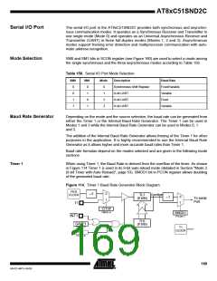
Asynchronous Modes
(Modes 1, 2 and 3)
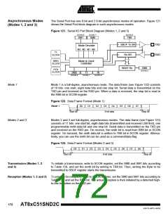
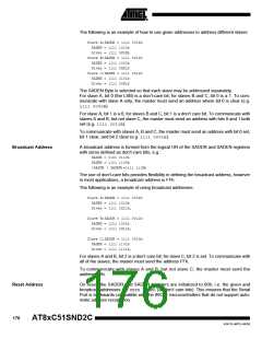
The Serial Port has one 8-bit and 2 9-bit asynchronous modes of operation. Figure 121
shows the Serial Port block diagram in such asynchronous modes.
Figure 121. Serial I/O Port Block Diagram (Modes 1, 2 and 3)
SCON.6
SCON.7
SCON.3
SM1
SM0
TB8
SBUF Tx SR
Rx SR
TXD
RXD
Mode Decoder
M3 M2 M1 M0
T1
CLOCK
IBRG
CLOCK
Mode & Clock
Controller
SBUF Rx
RB8
SCON.2
PER
CLOCK
SM2
SCON.4
TI
SCON.1
RI
SCON.0
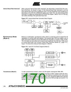
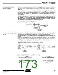
Mode 1
Mode 1 is a full-duplex, asynchronous mode. The data frame (see Figure 122) consists
of 10 bits: one start, eight data bits and one stop bit. Serial data is transmitted on the
TXD pin and received on the RXD pin. When a data is received, the stop bit is read in
the RB8 bit in SCON register.
Figure 122. Data Frame Format (Mode 1)
Mode 1
D0
D1
D2
D3
D4
D5
D6
D7
Start bit
8-bit data
Stop bit
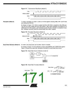
Modes 2 and 3
Modes 2 and 3 are full-duplex, asynchronous modes. The data frame (see Figure 123)
consists of 11 bits: one start bit, eight data bits (transmitted and received LSB first), one
programmable ninth data bit and one stop bit. Serial data is transmitted on the TXD pin
and received on the RXD pin. On receive, the ninth bit is read from RB8 bit in SCON
register. On transmit, the ninth data bit is written to TB8 bit in SCON register. Alterna-
tively, you can use the ninth bit can be used as a command/data flag.
Figure 123. Data Frame Format (Modes 2 and 3)
D0
D1
D2
D3
D4
D5
D6
D7
D8
Start bit
9-bit data
Stop bit
Transmission (Modes 1, 2
and 3)
To initiate a transmission, write to SCON register, set the SM0 and SM1 bits according
to Table 158, and set the ninth bit by writing to TB8 bit. Then, writing the Byte to be
transmitted to SBUF register starts the transmission.
Reception (Modes 1, 2 and 3)
To prepare for reception, write to SCON register, set the SM0 and SM1 bits according to
Table 158, and set the REN bit. The actual reception is then initiated by a detected high-
to-low transition on the RXD pin.
172
AT8xC51SND2C
4341D–MP3–04/05

 ATMEL [ ATMEL ]