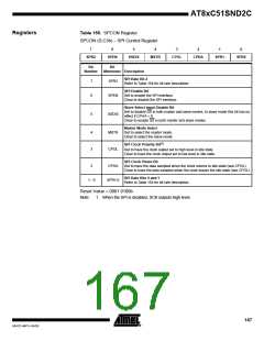
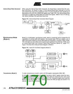
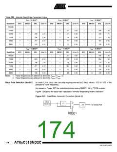
Internal Baud Rate Generator When using the Internal Baud Rate Generator, the Baud Rate is derived from the over-
flow of the timer. As shown in Figure 115 the Internal Baud Rate Generator is an 8-bit
auto-reload timer fed by the peripheral clock or by the peripheral clock divided by 6
depending on the SPD bit in BDRCON register (see Table 164). The Internal Baud Rate
Generator is enabled by setting BBR bit in BDRCON register. SMOD1 bit in PCON reg-
ister allows doubling of the generated baud rate.
Figure 115. Internal Baud Rate Generator Block Diagram
PER
CLOCK
÷ 6
0
1
Overflow
BRG
(8 bits)
÷ 2
0
1
To serial
Port
SPD
BDRCON.1
BRR
BDRCON.4
SMOD1
PCON.7
BRL
(8 bits)
IBRG
CLOCK
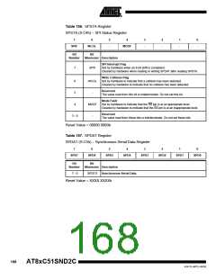
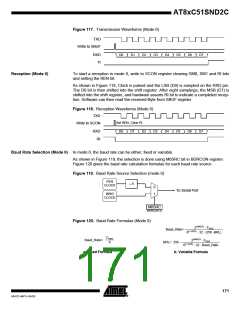
Synchronous Mode
(Mode 0)
Mode 0 is a half-duplex, synchronous mode, which is commonly used to expand the I/0
capabilities of a device with shift registers. The transmit data (TXD) pin outputs a set of
eight clock pulses while the receive data (RXD) pin transmits or receives a Byte of data.
The 8-bit data are transmitted and received least-significant bit (LSB) first. Shifts occur
at a fixed Baud Rate (see Section "Baud Rate Selection (Mode 0)", page 171).
Figure 116 shows the serial port block diagram in Mode 0.
Figure 116. Serial I/O Port Block Diagram (Mode 0)
SCON.6
SCON.7
SM1
SM0
SBUF Tx SR
SBUF Rx SR
RXD
Mode Decoder
M3 M2 M1 M0
Mode
Controller
PER
CLOCK
Baud Rate
Controller
TI
SCON.1
RI
SCON.0
TXD
BRG
CLOCK
Transmission (Mode 0)
To start a transmission mode 0, write to SCON register clearing bits SM0, SM1.
As shown in Figure 117, writing the Byte to transmit to SBUF register starts the trans-
mission. Hardware shifts the LSB (D0) onto the RXD pin during the first clock cycle
composed of a high level then low level signal on TXD. During the eighth clock cycle the
MSB (D7) is on the RXD pin. Then, hardware drives the RXD pin high and asserts TI to
indicate the end of the transmission.
170
AT8xC51SND2C
4341D–MP3–04/05

 ATMEL [ ATMEL ]