AS5050
Datasheet - Absolute Maximum Ratings
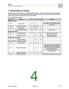
5 Absolute Maximum Ratings
Stresses beyond those listed in Table 2 may cause permanent damage to the device. These are stress ratings only, and functional operation of
the device at these or any other conditions beyond those indicated in Electrical Characteristics on page 5 is not implied. Exposure to absolute
maximum rating conditions for extended periods may affect device reliability.
Table 2. Absolute Maximum Ratings
Symbol
Parameter
Min
Max
Units
Comments
Electrical Parameters
Value of these process dependent parameters
are according to Process Parameter document,
current version
VDD
DC supply voltage
-0.3
5.0
V
VDDp
Peripheral supply voltage
Input pin voltage
-0.3
-0.3
-100
VDD+0.3
5.0
V
V
VIN
Iscr
Input current (latchup immunity)
100
mA
Norm: Jedec 78
Electrostatic Discharge
ESD
Electrostatic discharge
Package thermal resistance
±1
-
-
kV
Norm: MIL 883 E method 3015
Velocity=0, Multi Layer PCB;
Jedec Standard Testboard
ΘJA
33.5
°C/W
Continuous Power Dissipation
Pt
Temperature Ranges and Storage Conditions
Total power dissipation
36
mW
°C
Tstrg
Storage temperature
-55
125
The reflow peak soldering temperature (body
temperature) specified is in accordance with
IPC/JEDEC J-STD-020 “Moisture/Reflow
Sensitivity Classification for Non-Hermetic Solid
State Surface Mount Devices”.
TBODY
Package body temperature
260
85
°C
%
The lead finish for Pb-free leaded packages is
matte tin (100% Sn).
Humidity non-condensing
Moisture Sensitive Level
5
MSL
3
Represents a maximum floor life time of 168h
www.ams.com/AS5050
Revision 1.16
4 - 25

 AMSCO [ AMS(艾迈斯) ]