AS5050
Datasheet - Pin Assignments
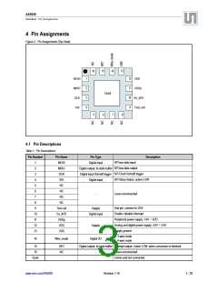
4 Pin Assignments
Figure 2. Pin Assignments (Top View)
16
15
14
13
1
2
3
4
12
11
10
9
MOSI
MISO
SCK
SS/
VDD
VDDp
Epad
En_INT/
Test_coil
5
6
7
8
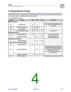
4.1 Pin Descriptions
Table 1. Pin Descriptions
Pin Number
Pin Name
MOSI
MISO
SCK
Pin Type
Description
SPI bus data input
1
2
Digital input
SPI bus data output
SPI Clock Schmitt trigger
Digital output, tri-state buffer
Digital input Schmitt trigger
Digital input
3
SPI Slave Select, active LOW
4
SS/
5
NC
6
NC
Leave unconnected
-
7
NC
8
NC
Test pin, connect to VSS
9
Test coil
En_INT/
VDDp
VDD
Supply
Enable / disable Interrupt
10
11
12
13
Digital input
Peripheral power supply, 1.8V ~ VDD
Analog and digital power supply, 3.0V ~ 3.6V
Supply ground
Supply
VSS
0: 3-wire mode
1: 4-wire mode
14
Wire_mode
Digital I/O
Interrupt output. Active LOW, when conversion is finished
Leave unconnected
15
16
INT/
NC
-
Digital output, tri-state buffer
-
-
Center pad not connected
Epad
www.ams.com/AS5050
Revision 1.16
3 - 25

 AMSCO [ AMS(艾迈斯) ]