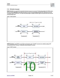
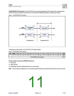
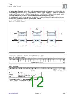
AS5050
Datasheet - Detailed Description
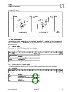
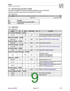
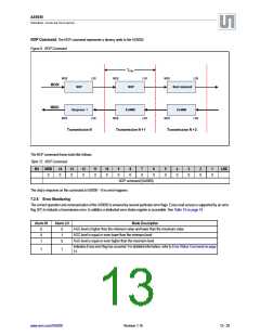
7.2.3 Write Data Package (Value Written to AS5050)
The write frame is compatible to the read frame and contains two additional bits, the don’t care and parity flag.
If the previous command was a write command a second package has to be transmitted.
Table 8. Write Package
Bit
MSB
14
13
12
11
10
9
8
7
6
5
4
3
2
1
LSB
Data <13:0>
Don’t care PAR
Bit
Description
Data
PAR
14-bit data to write to former selected address
Parity bit (EVEN)
7.2.4 Register Block
Table 9. Register Block
Register
Bit
Mode
Reset Value
Bit
Description
Power ON Reset (POR) Register - [0x3F22]
The POR cell is deactivated when the value 0x5A is written
to this register (30µA reduction of current consumption)
POR_OFF
8
R/W
0x00
<7:0>
Software Reset Register - [0x3C00]
software_reset 14
Master Reset Register - [0x33A5]
master_reset 14
Clear Error Flag Register - [0x3380]
clr_error_flag 14
No Operation Register - [0x0000]
NOP 14
Refer to SOFTWARE RESET Command on page 12
Inject a power on reset cycle
W
W
R
0x000
0x000
0x000
0x000
<13:0>
<13:0>
<13:0>
<13:0>
Refer to CLEAR ERROR FLAG Command on page 11
Refer to NOP Command on page 13
W
Automatic Gain Control (AGC) Register - [0x03FF8]
Automatic gain control:
low values = strong magnetic field
high values = weak magnetic field
AGC
6
R/W
0x20
<5:0>
Angular Data - [0x3FFF]
Measured angular value, 10-bit
Angle Value
10
1
R
R
0x000
0
<9:0>
<12>
Alarm bit indicating a too high magnetic field, active HIGH.
Refer to Error Monitoring on page 13
Alarm LO
Alarm HI
Alarm bit indicating a too low magnetic field, active HIGH.
Refer to Error Monitoring on page 13
1
R
R
0
<13>
Error Status Register - [0x335A]
error_status 14
Refer to Error Status Command on page 14
0x000
<13:0>
System Configuration Register 1 - [0x3F20]
‘01’ indicates 10-bit resolution
Silicon version 001
resolution
Chip_ID
2
3
R
R
‘01’
<13:12>
<11:9>
‘001’
www.ams.com/AS5050
Revision 1.16
9 - 25

 AMSCO [ AMS(艾迈斯) ]