AD7485
0
0
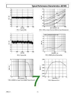
fIN = 10.7kHz
SNR = 78.76dB
SNR + D = 78.70dB
THD = –97.10dB
fIN = 507.3kHz
SNR = 78.35dB
SNR + D = 78.33dB
THD = –100.33dB
–20
–20
–40
–60
–80
–40
–60
–80
–100
–120
–140
–100
–120
–140
0
100
200
300
400
500
0
100
200
300
400
500
FREQUENCY – kHz
FREQUENCY – kHz
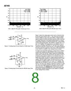
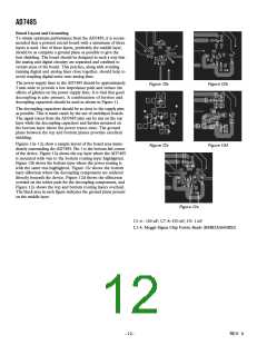
TPC 8. 64k FFT Plot with 500 kHz Input Tone
TPC 7. 64k FFT Plot with 10 kHz Input Tone
+V
S
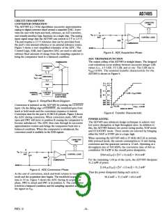
Figure 1 shows the analog input circuit used to obtain the data
for the FFT plot shown in TPC 7. The circuit uses an Analog
Devices AD829 op amp as the input buffer. A bipolar analog
signal is applied as shown and biased up with a stable, low noise
dc voltage connected to the labeled terminal shown. A 220 pF
compensation capacitor is connected between Pin 5 of the AD829
and the analog ground plane. The AD829 is supplied with +12 V
and –12 V supplies. The supply pins are decoupled as close to
the device as possible, with both a 0.1 µF and 10 µF capacitor
connected to each pin. In each case, the 0.1 µF capacitor should be
the closer of the two capacitors to the device. More information
on the AD829 is available on the Analog Devices website.
8
1kꢂ
1kꢂ
100ꢂ
AC
7
+
–
3
2
SIGNAL
V
6
IN
AD829
BIAS
VOLTAGE
4
5
1
–V
S
220pF
150ꢂ
Figure 1. Analog Input Circuit Used for 10 kHz Input Tone
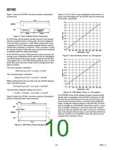
For higher input bandwidth applications, Analog Devices’ AD8021
op amp (also available as a dual AD8022) is the recommended
choice to drive the AD7485. Figure 2 shows the analog input
circuit used to obtain the data for the FFT plot shown in TPC 8.
A bipolar analog signal is applied to the terminal shown and
biased with a stable, low noise dc voltage connected as shown. A
10 pF compensation capacitor is connected between Pin 5 of the
AD8021 and the negative supply. As with the previous circuit,
the AD8021 is supplied with +12 V and –12 V supplies. The
supply pins are decoupled as close to the device as possible with
both a 0.1 µF and 10 µF capacitor connected to each pin. In each
case, the 0.1 µF capacitor should be the closer of the two capaci-
tors to the device. The AD8021 Logic Reference pin is tied to
analog ground and the DISABLE pin is tied to the positive sup-
ply as shown. Detailed information on the AD8021 is available
on the Analog Devices website.
+V
S
8
50ꢂ
AC
7
2
3
+
SIGNAL
V
6
IN
AD8021
220ꢂ
BIAS
VOLTAGE
4
–
5
1
10pF
–V
S
220ꢂ
10pF
Figure 2. Analog Input Circuit Used for 500 kHz Input Tone
–8–
REV. 0

 AMICC [ AMIC TECHNOLOGY ]