AD7485
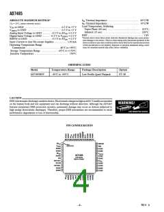
ABSOLUTE MAXIMUM RATINGS*
(TA = 25°C, unless otherwise noted.)
ꢂJA Thermal Impedance . . . . . . . . . . . . . . . . . . . . . . . 50°C/W
ꢂJC Thermal Impedance . . . . . . . . . . . . . . . . . . . . . . . 10°C/W
Lead Temperature, Soldering
Vapor Phase (60 sec) . . . . . . . . . . . . . . . . . . . . . . . . 215°C
Infrared (15 sec) . . . . . . . . . . . . . . . . . . . . . . . . . . . 220°C
ESD . . . . . . . . . . . . . . . . . . . . . . . . . . . . . . . . . . . . . . . . . 1 kV
*Stresses above those listed under Absolute Maximum Ratings may cause perma-
nent damage to the device. This is a stress rating only; functional operation of the
device at these or any other conditions above those listed in the operational sections
of this specification is not implied. Exposure to absolute maximum rating condi-
tions for extended periods may affect device reliability.
VDD to GND . . . . . . . . . . . . . . . . . . . . . . . . . . –0.3 V to +7 V
VDRIVE to GND . . . . . . . . . . . . . . . . . . . . . . . . –0.3 V to +7 V
Analog Input Voltage to GND . . . . . . –0.3 V to AVDD + 0.3 V
Digital Input Voltage to GND . . . . . –0.3 V to VDRIVE + 0.3 V
REFIN to GND . . . . . . . . . . . . . . . . –0.3 V to AVDD + 0.3 V
Input Current to Any Pin except Supplies . . . . . . . . . 10 mA
Operating Temperature Range
Commercial . . . . . . . . . . . . . . . . . . . . . . . . –40°C to +85°C
Storage Temperature Range . . . . . . . . . . . . –65°C to +150°C
Junction Temperature . . . . . . . . . . . . . . . . . . . . . . . . . 150°C
ORDERING GUIDE
Model
Temperature Range
–40°C to +85°C
Package Description
Option
AD7485BST
Low Profile Quad Flatpack
ST-48
CAUTION
ESD (electrostatic discharge) sensitive device. Electrostatic charges as high as 4000 V readily accumulate
on the human body and test equipment and can discharge without detection. Although the AD7485
features proprietary ESD protection circuitry, permanent damage may occur on devices subjected to
high energy electrostatic discharges. Therefore, proper ESD precautions are recommended to avoid
performance degradation or loss of functionality.
WARNING!
ESD SENSITIVE DEVICE
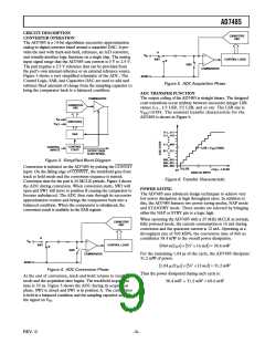
PIN CONFIGURATION
48 47 46 45 44 43 42 41 40 39 38 37
1
AV
DD
36
35
34
33
32
31
30
29
28
27
26
25
SMODE
PIN 1
IDENTIFIER
2
3
C
BIAS
TFS
DGND
DGND
AGND
4
AGND
5
AV
DD
AGND
VIN
V
DRIVE
AD7485
6
DGND
DGND
TOP VIEW
7
(Not to Scale)
8
REFOUT
REFIN
REFSEL
AGND
DV
DD
9
DGND
DGND
DGND
DGND
10
11
12
AGND
13 14 15 16 17 18 19 20 21 22 23 24
–4–
REV. 0

 AMICC [ AMIC TECHNOLOGY ]