AD7485
CIRCUIT DESCRIPTION
CONVERTER OPERATION
CAPACITIVE
DAC
The AD7485 is a 14-bit algorithmic successive-approximation
analog-to-digital converter based around a capacitive DAC. It pro-
vides the user with track-and-hold, reference, an A/D converter,
and versatile interface logic functions on a single chip. The analog
input signal range that the AD7485 can convert is 0 V to 2.5 V.
The part requires a 2.5 V reference that can be provided from
the part’s own internal reference or an external reference source.
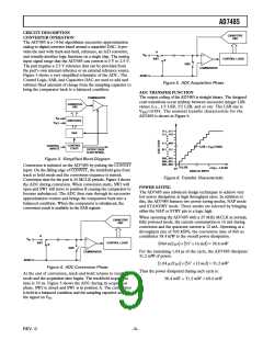
Figure 3 shows a very simplified schematic of the ADC. The
Control Logic, SAR, and Capacitive DAC are used to add and
subtract fixed amounts of charge from the sampling capacitor to
bring the comparator back to a balanced condition.
A
V
IN
+
SW1
CONTROL LOGIC
B
–
SW2
COMPARATOR
AGND
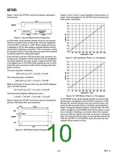
Figure 5. ADC Acquisition Phase
ADC TRANSFER FUNCTION
The output coding of the AD7485 is straight binary. The designed
code transitions occur midway between successive integer LSB
values (i.e., 1/2 LSB, 3/2 LSB, and so on). The LSB size is
VREF/16384. The nominal transfer characteristic for the
AD7485 is shown in Figure 6.
COMPARATOR
CAPACITIVE
DAC
V
IN
SWITCHES
SAR
V
REF
111...111
111...110
111...000
CONTROL
LOGIC
CONTROL
INPUTS
1LSB =V
/16384
REF
011...111
OUTPUT DATA
14-BIT SERIAL
000...010
000...001
000...000
Figure 3. Simplified Block Diagram
Conversion is initiated on the AD7485 by pulsing the CONVST
input. On the falling edge of CONVST, the track/hold goes from
track to hold mode and the conversion sequence is started.
Conversion time for the part is 24 MCLK periods. Figure 4 shows
the ADC during conversion. When conversion starts, SW2 will
open and SW1 will move to position B causing the comparator to
become unbalanced. The ADC then runs through its successive
approximation routine and brings the comparator back into a
balanced condition. When the comparator is rebalanced, the
conversion result is available in the SAR register.
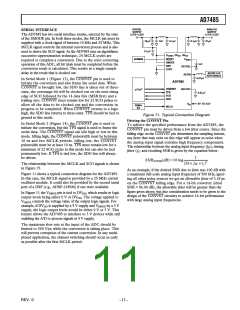
0.5LSB
+V
REF
–1.5LSB
0V
ANALOG INPUT
Figure 6. Transfer Characteristic
POWER SAVING
The AD7485 uses advanced design techniques to achieve very
low power dissipation at high throughput rates. In addition to
this, the AD7485 features two power saving modes, NAP mode
and STANDBY mode. These modes are selected by bringing
either the NAP or STBY pin to a logic high.
When operating the AD7485 with a 25 MHz MCLK in normal,
fully powered mode, the current consumption is 16 mA during
conversion and the quiescent current is 12 mA. Operating at a
throughput rate of 500 kSPS, the conversion time of 960 ns
contributes 38.4 mW to the overall power dissipation.
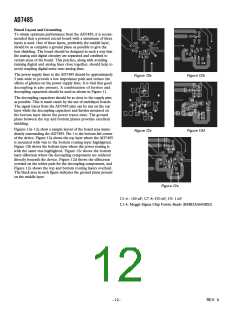
CAPACITIVE
DAC
A
V
IN
+
SW1
CONTROL LOGIC
960 ns/2 ꢀs × 5V ×16 mA = 38.4 mW
(
)
(
)
B
–
SW2
COMPARATOR
For the remaining 1.04 µs of the cycle, the AD7485 dissipates
31.2 mW of power.
AGND
1.04 ꢀs/2 ꢀs × 5V ×12 mA = 31.2 mW
(
)
(
)
Figure 4. ADC Conversion Phase
Thus the power dissipated during each cycle is:
At the end of conversion, track-and-hold returns to tracking
mode and the acquisition time begins. The track/hold acquisition
time is 70 ns. Figure 5 shows the ADC during its acquisition
phase. SW2 is closed and SW1 is in position A. The comparator
is held in a balanced condition and the sampling capacitor acquires
the signal on VIN.
38.4 mW + 31.2 mW = 69.6 mW
REV. 0
–9–

 AMICC [ AMIC TECHNOLOGY ]