AD7485
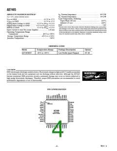
PIN FUNCTION DESCRIPTIONS
Pin
No.
1, 5, 13, 46
2
Mnemonic
AVDD
CBIAS
Description
Positive Power Supply for Analog Circuitry
Decoupling Pin for Internal Bias Voltage. A 1 nF capacitor should be placed between this pin
and AGND.
3, 4, 6, 11, 12,
14, 15, 47, 48
AGND
Power Supply Ground for Analog Circuitry
7
8
VIN
REFOUT
Analog Input. Single-ended analog input channel.
Reference Output. REFOUT connects to the output of the internal 2.5 V reference buffer. A 470 nF
capacitor must be placed between this pin and AGND.
9
REFIN
Reference Input. A 470 nF capacitor must be placed between this pin and AGND. When using
an external voltage reference source, the reference voltage should be applied to this pin.
10
REFSEL
Reference Decoupling Pin. When using the internal reference, a 1 nF capacitor must be connected
from this pin to AGND. When using an external reference source, this pin should be connected
directly to AGND.
16
17
18
STBY
NAP
Standby Logic Input. When this pin is logic high, the device will be placed in STANDBY mode.
See the Power Saving section for further details.
Nap Logic Input. When this pin is logic high, the device will be placed in a very low power mode.
See the Power Saving section for further details.
Master Clock Input. This is the input for the master clock, which controls the conversion cycle. The fre-
quency of this clock may be up to 25 MHz. Twenty-four clock cycles are required for each conversion.
Ground Reference for Digital Circuitry
MCLK
DGND
19, 20, 22–28
30, 31, 33, 34
37–39, 43, 44
21
SDO
Serial Data Output. The conversion data is latched out on this pin on the rising edge of SCO. It
should be latched into the receiving serial port of the DSP on the falling edge of SCO. The over-
range bit is latched out first, then 14 bits of data (MSB first) followed by a trailing zero.
29, 45
32
DVDD
VDRIVE
Positive Power Supply for Digital Circuitry
Logic Power Supply Input. The voltage supplied at this pin determines at what voltage the interface
logic of the AD7485 will operate.
35
TFS
Transmit Frame Sync Input. In Serial Mode 2, this pin acts as a framing signal for the serial data
being clocked out on SDO. A falling edge on TFS brings SDO out of three-state and the data starts
to get clocked out on the next rising edge of SCO.
36
40
41
42
SMODE
SCO
Serial Mode Input. A logic low on this pin selects Serial Mode 1 and a logic high selects Serial
Mode 2. See the Serial Interface section for further details.
Serial Clock Output. This clock is derived from MCLK and is used to latch conversion data from
the device. See the Serial Interface section for further details.
Convert Start Logic Input. A conversion is initiated on the falling edge of the CONVST signal. The
input track/hold amplifier goes from track mode to hold mode and the conversion process commences.
CONVST
RESET
Reset Logic Input. A falling edge on this pin resets the internal state machine and terminates a
conversion that may be in progress. Holding this pin low keeps the part in a reset state.
REV. 0
–5–

 AMICC [ AMIC TECHNOLOGY ]