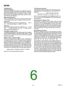
AD7485
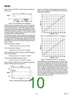
Figure 7 shows the AD7485 conversion sequence operating in
normal mode.
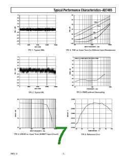
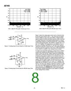
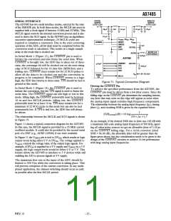
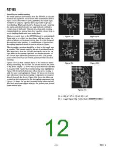
Figures 9 and 10 show a typical graphical representation of
power versus throughput for the AD7485 when in normal and
NAP modes, respectively.
2ꢀs
80
78
76
74
72
70
68
66
64
62
60
CONVST
READ DATA
960ns
CONVERSION
FINISHED
TFS
1.04ꢀs
Figure 7. Normal Mode Power Dissipation
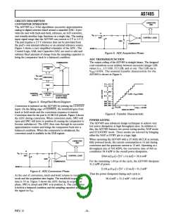
In NAP mode, all the internal circuitry except for the internal
reference is powered down. In this mode, the power dissipation
of the AD7485 is reduced to 3 mW. When exiting NAP mode,
a minimum of 300 ns when using an external reference must be
waited before initiating a conversion. This is necessary to allow
the internal circuitry to settle after power-up and for the track/hold
to properly acquire the analog input signal.
0
100 200 300 400 500 600 700 800 900 1000
THROUGHPUT – kSPS
If the AD7485 is put into NAP mode after each conversion, the
average power dissipation will be reduced but the throughput
rate will be limited by the power-up time. Using the AD7485 with
a throughput rate of 100 kSPS while placing the part in NAP
mode after each conversion would result in average power dissi-
pation as follows:
Figure 9. Normal Mode, Power vs. Throughput
50
45
40
35
30
25
20
15
10
5
The power-up phase contributes:
300 ns/10 ꢀs × 5V ×12 mA = 1.8 mW
(
)
(
)
The conversion phase contributes:
960 ns/10 ꢀs × 5V ×16 mA = 7.68 mW
(
)
(
)
While in NAP mode for the rest of the cycle, the AD7485 dissipates
only 2.185 mW of power.
8.74 ꢀs/10 ꢀs × 5V × 0.6 mA = 2.622 mW
0
(
)
(
)
0
50
100 150 200 250 300 350 400 450 500
THROUGHPUT – kSPS
Thus the power dissipated during each cycle is:
Figure 10. NAP Mode, Power vs. Throughput
1.8 mW + 7.68 mW + 2.622 mW + 12.1mW
In STANDBY mode, all the internal circuitry is powered down
and the power consumption of the AD7485 is reduced to 10 µW.
Because the internal reference has been powered down, the
power-up time necessary before a conversion can be initiated is
longer. If using the internal reference of the AD7485, the ADC
must be brought out of STANDBY mode 500 ms before a conver-
sion is initiated. Initiating a conversion before the required
power-up time has elapsed will result in incorrect conversion
data. If an external reference source is used and kept powered up
while the AD7485 is in STANDBY mode, the power-up time
required will be reduced to 80 µs.
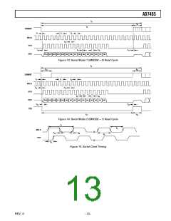
Figure 8 shows the AD7485 conversion sequence if putting the
part into NAP mode after each conversion.
1.26ꢀs
8.74ꢀs
NAP
CONVST
TFS
300ns
10ꢀs
Figure 8. NAP Mode Power Dissipation
–10–
REV. 0

 AMICC [ AMIC TECHNOLOGY ]