AD7485
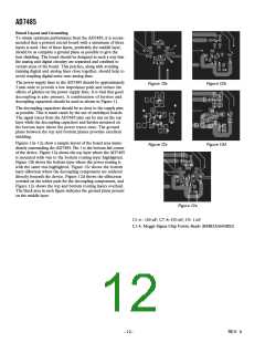
Board Layout and Grounding
To obtain optimum performance from the AD7485, it is recom-
mended that a printed circuit board with a minimum of three
layers is used. One of these layers, preferably the middle layer,
should be as complete a ground plane as possible to give the
best shielding. The board should be designed in such a way that
the analog and digital circuitry are separated and confined to
certain areas of the board. This practice, along with avoiding
running digital and analog lines close together, should help to
avoid coupling digital noise onto analog lines.
The power supply lines to the AD7485 should be approximately
3 mm wide to provide a low impedance path and reduce the
effects of glitches on the power supply lines. It is vital that good
decoupling is also present. A combination of ferrites and
decoupling capacitors should be used as shown in Figure 11.
Figure 12a
Figure 12b
The decoupling capacitors should be as close to the supply pins
as possible. This is made easier by the use of multilayer boards.
The signal traces from the AD7485 pins can be run on the top
layer while the decoupling capacitors and ferrites mounted on
the bottom layer where the power traces exist. The ground
plane between the top and bottom planes provides excellent
shielding.
Figures 12a–12e show a sample layout of the board area imme-
diately surrounding the AD7485. Pin 1 is the bottom left corner
of the device. Figure 12a shows the top layer where the AD7485
is mounted with vias to the bottom routing layer highlighted.
Figure 12b shows the bottom layer where the power routing is
with the same vias highlighted. Figure 12c shows the bottom
layer silkscreen where the decoupling components are soldered
directly beneath the device. Figure 12d shows the silkscreen
overlaid on the solder pads for the decoupling components, and
Figure 12e shows the top and bottom routing layers overlaid.
The black area in each figure indicates the ground plane present
on the middle layer.
Figure 12c
Figure 12d
Figure 12e
C1-6 : 100 nF, C7–8: 470 nF, C9: 1 nF
L1-4: Meggit-Sigma Chip Ferrite Beads (BMB2A0600RS2)
–12–
REV. 0

 AMICC [ AMIC TECHNOLOGY ]