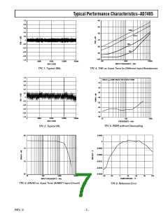
AD7485
DIGITAL
SUPPLY
4.75V–5.25V
ANALOG
SUPPLY
4.75V–5.25V
SERIAL INTERFACE
The AD7485 has two serial interface modes, selected by the state
of the SMODE pin. In both these modes, the MCLK pin must be
supplied with a clock signal of between 10 kHz and 25 MHz. This
MCLK signal controls the internal conversion process and is also
used to derive the SCO signal. As the AD7485 uses an algorithmic
successive-approximation technique, 24 MCLK cycles are
required to complete a conversion. Due to the error-correcting
operation of this ADC, all bit trials must be completed before the
conversion result is calculated. This results in a single sample
delay in the result that is clocked out.
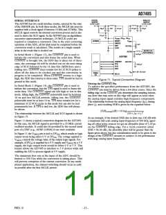
+
+
10ꢀF
1nF
0.1ꢀF
0.1ꢀF
47ꢀF
0.1ꢀF
V
DV
AV
DRIVE
DD DD
C
ADM809
RESET
SMODE
NAP
BIAS
1nF
REFSEL
REFIN
STBY
AD780 2.5V
REFERENCE
0.47ꢀF
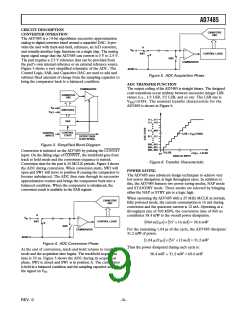
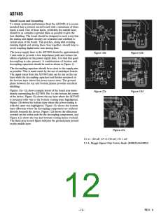
In Serial Mode 1 (Figure 13), the CONVST pin is used to
initiate the conversion and also frame the serial data. When
CONVST is brought low, the SDO line is taken out of three-
state, the overrange bit will be clocked out on the next rising
edge of SCO followed by the 14 data bits (MSB first) and a
trailing zero. CONVST must remain low for 22 SCO pulses to
allow all the data to be clocked out and the conversion in
progress to be completed. When CONVST returns to a logic
high, the SDO line returns to three-state. TFS should be tied to
ground in this mode.
AD7485
CONVST
REFOUT
ꢀC/ꢀP
TFS
SCO
SDO
0.47ꢀF
V
0V TO 2.5V
IN
25MHz
XO
MCLK
Figure 11. Typical Connection Diagram
Driving the CONVST Pin
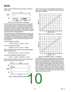
In Serial Mode 2 (Figure 14), the CONVST pin is used to
initiate the conversion, but the TFS signal is used to frame the
serial data. The CONVST signal can idle high or low in this
mode. Idling high, the CONVST pulsewidth must be between
10 ns and two MCLK periods. Idling low, the CONVST
pulsewidth must be at least 10 ns. TFS must remain low for a
minimum of 22 SCO cycles in this mode but can also be tied
permanently low. If TFS is tied low, the SDO line will always
be driven.
To achieve the specified performance from the AD7485, the
CONVST pin must be driven from a low jitter source. Since the
falling edge on the CONVST pin determines the sampling instant,
any jitter that may exist on this edge will appear as noise when
the analog input signal contains high frequency components.
The relationship between the analog input frequency (fIN), timing
jitter (tj), and resulting SNR is given by the equation below.
1
SNRJITTER(dB) = 10 log
(2π × fIN × tj )2
The relationship between the MCLK and SCO signals is shown
in Figure 15.
As an example, if the desired SNR due to jitter was 100 dB with
a maximum full-scale analog input frequency of 500 kHz, ignor-
ing all other noise sources we get an allowable jitter of 3.18 ps
on the CONVST falling edge. For a 14-bit converter (ideal
SNR = 86.04 dB), the allowable jitter will be greater than the
figure given above; but due consideration needs to be given to the
design of the CONVST circuitry to achieve 14-bit performance
with large analog input frequencies.
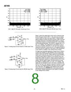
Figure 11 shows a typical connection diagram for the AD7485.
In this case, the MCLK signal is provided by a 25 MHz crystal
oscillator module. It could also be provided by the second serial
port of a DSP (e.g., ADSP-2189M) if one were available.
In Figure 11 the VDRIVE pin is tied to DVDD, which results in logic
output levels being either 0 V or DVDD. The voltage applied to
VDRIVE controls the voltage value of the output logic signals. For
example, if DVDD is supplied by a 5 V supply and VDRIVE by a 3 V
supply, the logic output levels would be either 0 V or 3 V. This
feature allows the AD7485 to interface to 3 V devices while still
enabling the A/D to process signals at 5 V supply.
The maximum slew rate at the input of the ADC should be
limited to 500 V/µs while the conversion is taking place. This
will prevent corruption of the current conversion. In any multi-
plexed application, the channel switching should occur as early
as possible after the first MCLK period.
REV. 0
–11–

 AMICC [ AMIC TECHNOLOGY ]