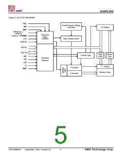
A49FL004
GENERAL DESCRIPTION
The A49FL004 is a 4 Mbit 3.0 Volt-only Flash Memories used
for BIOS storage in PCs and Notebooks. This device is
designed to use a single low voltage, ranging from 3.0 Volt to
3.6 Volt, power supply to perform in-system or off-system
read, erase and program operations. The device conforms to
Intel® Low Pin Count (LPC) Interface specification revision
1.1 and also is compatible with Intel 82802 Firmware Hub
(FWH) for most PC and Notebook applications. The
A49FL004 supports two configurable interfaces: In-system
hardware interface which can automatic detect the FWH or
LPC memory cycle for in-system read and write operations,
and Address/Address Multiplexed (A/A Mux) interface for fast
manufacturing on EPROM Programmers. This device is
designed to work with both Intel Family chipset and Non-Intel
Family Chipset, it will provide PC and Notebook
manufacturers great flexibility and simplicity for design,
procurement, and material inventory.
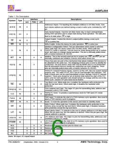
The program operation of A49FL004 is executed by issuing
the program command code into command register. The
internal control logic automatically handles the programming
voltage ramp-up and timing. The erase operation of the
device is also executed by issuing the sector, block, or chip
erase command code into command register. The internal
control logic automatically handles the erase voltage ramp-
up and timing. The device offer Data Polling and Toggle Bit
functions in FWH/LPC and A/A Mux modes, the progress or
completion of program and erase operation can be detected
by reading the Data Polling on I/O7 or Toggle Bit on I/O6.
The A49FL004 has a 64 KByte top boot block. The boot
block can be write protected by a hardware method
controlled by the TBL pin or a register-based protection
turned on/off by the Block Locking Registers (FWH or LPC
mode only). The rest of blocks except boot block in the
The memory array of A49FL004 is divided into 128 uniform 4
KByte sectors or 8 uniform 64 KByte blocks (sector group -
consists of sixteen adjacent sectors). The sector or block
erase feature in the A49FL004 allows user to flexibly erase a
memory area as 4Kbyte or 64 KByte by one single erase
operation without affecting the data in others. The chip erase
feature allows the whole memory to be erased in one single
erase operation. The device can be programmed on a byte-
by-byte basis after performing the erase operation.
device also can be write protected by WP pin or Block
Locking Registers (FWH or LPC mode only).
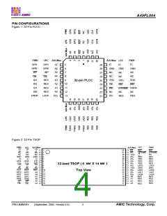
The A49FL004 is manufactured on AMIC ‘s advanced
nonvolatile technology. The device is offered in 32-pin TSOP
and PLCC packages with optional environmental friendly
lead-free package.
PRELIMINARY
(September, 2005, Version 0.0)
2
AMIC Technology, Corp.

 AMICC [ AMIC TECHNOLOGY ]