A49FL004
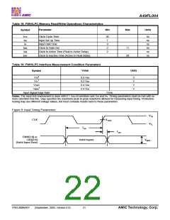
Table 18: FWH/LPC Memory Read/Write Operations Characteristics
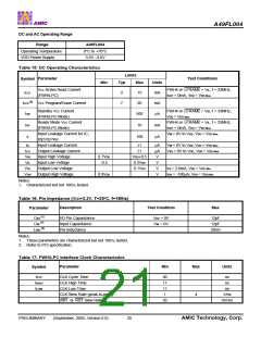
Parameter
Min
Max
Units
Symbol
tCYC
tSU
Clock Cycle Time
30
7
ns
ns
ns
ns
ns
ns
Input Set Up Time
tH
Input Hold Time
0
tVAL
tON
tOFF
Clock to Data Out
2
11
28
Clock to Active Time (Float to Active Delay)
Clock to Inactive Time (Active to Float Delay)
2
Table 19: FWH/LPC Interface Measurement Condition Parameters
Value
Units
Symbol
4
VTH
0.6 VDD
0.2 VDD
0.4 VDD
0.4 VDD
V
V
V
V
1
VTL
VTEST
1
VMAX
Input Signal Edge Rate
1V/ns
Notes: The input test environment is done with 0.1 VDD of overdrive over VIH and VIL. Timing parameters must be met with no
more overdrive that this. VMAX specifies the maximum peak-to-peak waveform allowed for measuring input timing. Production
testing may use different voltage values, but must correlate results back to these parameters.
Figure 9: Input Timing Parameters
VTH
CLK
VTEST
VTL
TSU
TDH
FWH[3:0] or
LAD[3:0]
Valid Inputs
VMAX
(Valid Input Data)
PRELIMINARY
(September, 2005, Version 0.0)
21
AMIC Technology, Corp.

 AMICC [ AMIC TECHNOLOGY ]