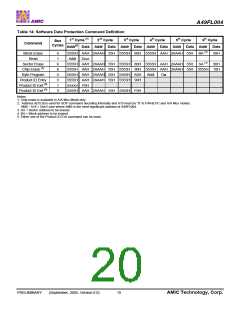
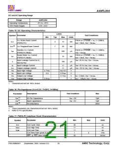
A49FL004
Table 20: FWH/LPC Interface AC Input/Output Characteristics
Parameter
Test Conditions
Min
Max
Units
Symbol
0 < VOUT ≤ 0.3VDD
0.3VDD < VOUT ≤ 0.9VDD
0.7VDD < VOUT ≤ VDD
VOUT = 0.7VDD
-12 VDD
mA
mA
IOH (AC)
Switching Current High
(Test Point)
-17.1(VDD-VOUT)
Equation C (1)
mA
-32 VDD
VDD > VOUT ≥ 0.6VDD
0.6VDD > VOUT > 0.1VDD
0.18VDD > VOUT > 0
VOUT=0.18VDD
16VDD
mA
mA
mA
IOL (AC)
Switching Current Low
-17.1(VDD – VOUT)
Equation D (1)
(Test Point)
38VDD
ICL
Low Clamp Current
High Clamp Current
Output Rise Slew Rate
Output Fall Slew Rate
-3 < VIN ≤ -1
-25+(VIN+1)/0.015
mA
mA
ICH
VDD+4 > VIN > VDD+1
0.2VDD-0.6VDD load
0.6VDD-0.2VDD load
25+(VIN-VDD-1)/0.015
slewr (2)
slewf (2)
1
1
4
4
V/ns
V/ns
Notes:
1. See PCI specification.
2. PCI specification output load is used.
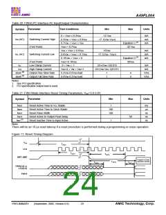
Table 21: FWH Mode Interface Reset Timing Parameters, VDD=3.0-3.6V
Parameter
Min
Max
Units
Symbol
tPRST
tKRST
tRSTP
tRSTF
Reset Active Time to VCC Stable
Reset Active Time to Clock Stable
Reset Pulse Width
1
ms
µs
ns
ns
ns
100
100
Reset Active to Output Float Delay
Reset Inactive Time to Input Active
50
(1)
tRST
1
Note:
There will be an 10 µs reset latency if a reset procedure is performed during a programming or erase operation.
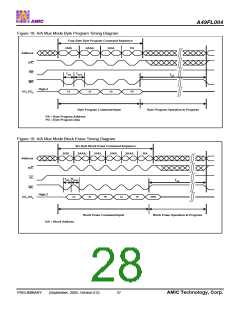
Figure 11: Reset Timing Diagram
VDD
TPRST
CLK
TKRST
TRSTP
RST / INIT
Program or Erase
TRSTE
Operation Aborted
TRSTF
TRST
FWH[3:0] or
LAD[3:0]
FWH4
PRELIMINARY
(September, 2005, Version 0.0)
23
AMIC Technology, Corp.

 AMICC [ AMIC TECHNOLOGY ]