A49FL004
A/A MUX MODE AC CHARACTERISTICS
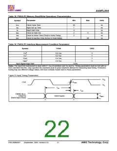
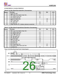
Table 22: A/A Mux Mode Read Operations Characteristics
Parameter
Min
Max
Units
Symbol
tRC
Read Cycle Time
270
1
ns
ms
ns
ns
ns
ns
ns
µs
ns
tRST
tAS
RST High to Row Address Setup Time
R/C Address Set-up Time
R/C Address Hold Time
45
45
tAH
tAA
Address to Output Delay
120
50
tOE
OE to Output Delay
tDF
OE Output High Z
0
50
0
30
tVCS
tOH
VDD Setup Time
Output Hold from OE or Address, whichever occurred first
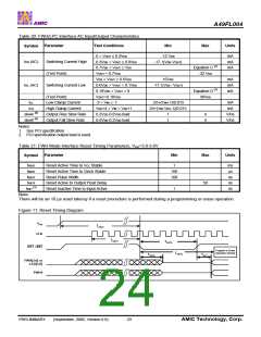
Table 21: A/A Mux Write (Program/Erase) Operations Characteristics
Parameter
Min
Max
Units
Symbol
tRST
tAS
RST High to Row Address Setup Time
R/C Address Setup Time
R/C Address Hold Time
R/C to WE High Time
OE High Setup Time
1
50
50
50
20
20
100
100
50
5
ms
ns
ns
ns
ns
ns
ns
ns
ns
ns
µs
ms
µs
tAH
tCWH
tOES
tOEH
tWP
tWPH
tDS
OE High Hold Time
Write Pulse Width
WE Pulse Width High
Data Setup Time
tDH
Data Hold Time
tBP
Byte Programming Time
Chip, Sector or Block Erase Cycle Time
VDD Setup Time
40
80
tEC
tVCS
50
Figure 14: A/A Mux Mode Read Cycle Timing Diagram
TRSTP
RST
TRST
TRC
Row Address
Column Address
Row Address
Column Address
Address
TAS
TAH
TAS
TAH
R/C
WE
VIH
TAA
TOH
OE
TOE
TOHZ
TOLZ
High-Z
High-Z
Data Valid
I/O7-I/O0
PRELIMINARY
(September, 2005, Version 0.0)
25
AMIC Technology, Corp.

 AMICC [ AMIC TECHNOLOGY ]