n BCR40
n BCR41
n BCR42
n BCR43
n BCR44
n BCR45
n BCR46
n BCR47
PCI DATA Register 3 (DATA3)
Alias Register
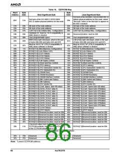
Note: The first bit out of any word location in the EE-
PROM is treated as the MSB of the register being pro-
grammed. For example, the first bit out of EEPROM
word location 09h will be written into BCR4, bit 15; the
second bit out of EEPROM word location 09h will be
written into BCR4, bit 14, etc.
PCI DATA Register 4 (DATA4)
Alias Register
PCI DATA Register 5 (DATA5)
Alias Register
There are two checksum locations within the EE-
PROM. The first checksum will be used by AMD driver
software to verify that the ISO 8802-3 (IEEE/ANSI
802.3) station address has not been corrupted. The
value of bytes 0Ch and 0Dh should match the sum of
bytes 00h through 0Bh and 0Eh and 0Fh. The second
checksum location (byte 51h) is not a checksum total,
but is, instead, a checksum adjustment. The value of
this byte should be such that the total checksum for the
entire 82 bytes of EEPROM data equals the value FFh.
The checksum adjust byte is needed by the controller
in order to verify that the EEPROM content has not
been corrupted.
PCI DATA Register 6 (DATA6)
Alias Register
PCI DATA Register 7 (DATA7)
Alias Register
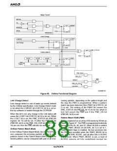
OnNow Pattern Matching
Register 1
OnNow Pattern Matching
Register 2
OnNow Pattern Matching
Register 3
n BCR48
n BCR49
n CRS12
n CRS13
n CRS14
n CSR116
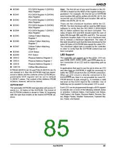
LED4 Status
LED Support
PHY Select
Physical Address Register 0
Physical Address Register 1
Physical Address Register 2
OnNow Miscellaneous
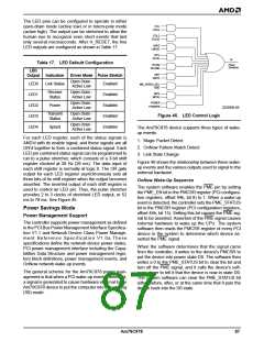
The controller can support up to five LEDs. LED out-
puts LED0, LED1, LED2, LED3, and LED4 allow for di-
rect connection of an LED and its supporting pull-up
device.
In applications that want to use the pin to drive an LED
and also have an EEPROM, it might be necessary to
buffer the LED3 circuit from the EEPROM connection.
When an LED circuit is directly connected to the
EEDO/LED3 pin, then it is not possible for most EE-
PROM devices to sink enough IOL to maintain a valid
low level on the EEDO input to the controller. Use of
buffering can be avoided if a low power LED is used.
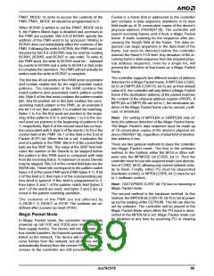
If PREAD (BCR19, bit 14) and PVALID (BCR19, bit 15)
are cleared to 0, then the EEPROM read has experi-
enced a failure and the contents of the EEPROM pro-
grammable BCR register will be set to default
H_RESET values. The content of the Address PROM
locations, however, will not be cleared.
EEPROM MAP
Each LED can be programmed through a BCR register
to indicate one or more of the following network status
or activities: Collision Status, Full-Duplex Link Status,
Half-Duplex Link Status, Receive Match, Receive Sta-
tus, Magic Packet, Disable Transceiver, Transmit Sta-
tus, Power, and Speed.
The automatic EEPROM read operation will access 41
words (i.e., 82 bytes) of the EEPROM. The format of
the EEPROM contents is shown in Table 16, beginning
with the byte that resides at the lowest EEPROM ad-
dress.
Am79C978
85

 AMD [ AMD ]