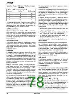
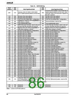
The start field (ST) is followed by the operation field
(OP). The operation field (OP) indicates whether the
operation is a read or a write operation. This is followed
by the PHY address (PHYAD) and the register address
(REGAD) that was programed into BCR33 of the Fast
Ethernet controller. This field is followed by a bus turn-
around field (TA). During the read operation, the bus
turnaround field is used to determine if the PHY is re-
sponding properly to the read request. The data field
to/from the MAC controller is then written to or read
from BCR34. The final field is the idle field, and it is re-
quired to allow the drivers to turn off.
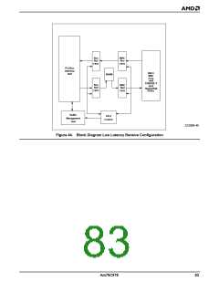
the controller will not configure for low latency receive
mode. The controller will provide a fast path on the re-
ceive side bypassing the SRAM. All transmit traffic will
go to the SRAM, so SRAM_BND (BCR26, bits 7-0) has
no meaning in low latency receive mode. When the
controller has received 16 bytes from the network, it will
start a DMA request to the PCI Bus Interface Unit. The
controller will not wait for the first 64 bytes to pass to
check for collisions in Low Latency Receive mode. The
controller must be in STOP before switching to this
mode. See Figure 44.
CAUTION: To provide data integrity when switching
into and out of the low latency mode, DO NOT SET the
FASTSPNDE bit when setting the SPND bit. Receive
frames WILL be overwritten and the controller may give
erratic behavior when it is enabled again.
The PHYADD field, which is five bits wide, allows 32
unique PHY addresses. The managed PHY layer de-
vice that is connected to a station management entity
via the MII interface has to respond to transactions ad-
dressed to the PHY’s address. A station management
entity attached to multiple PHYs is required to have
prior knowledge of the appropriate PHY address.
Direct SRAM Access
The SRAM can be accessed through the Expansion
Bus Data port (BCR30). To access this data port, the
user must load the upper address EPADDRU (BCR29,
bits 3-0) and set FLASH (BCR29, bit 15) to 0. Then the
user will load the lower 16 bits of address EPADDRL
(BCR28, bits 15-0). To initiate a read, the user reads
the Expansion Bus Data Port (BCR30). This slave ac-
cess from the PCI will result in a retry for the very first
access. Subsequent accesses may give a retry or not,
depending on whether or not the data is present and
valid. The direct SRAM access uses the same FLASH/
EPROM access except for accessing the SRAM in
word format instead of byte format. This access is
meant to be a diagnostic access only. The SRAM can
only be accessed while the controller is in STOP or
SPND (FASTSPNDE is set to 0) mode.
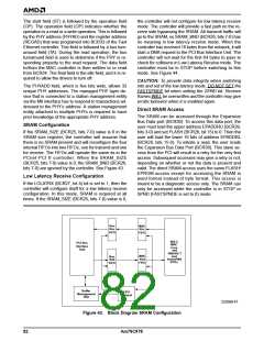
SRAM Configuration
If the SRAM_SIZE (BCR25, bits 7-0) value is 0 in the
SRAM size register, the controller will assume that
there is no SRAM present and will reconfigure the four
internal FIFOs into two FIFOs, one for transmit and one
for receive. The FIFOs will operate the same as in the
PCnet-PCI II controller. When the SRAM_SIZE
(BCR25, bits 7-0) value is 0, the SRAM_BND (BCR26,
bits 7-0) are ignored by the controller. See Figure 43.
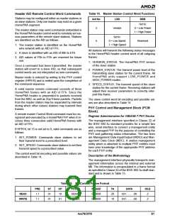
Low Latency Receive Configuration
If the LOLATRX (BCR27, bit 4) bit is set to 1, then the
controller will configure itself for a low latency receive
configuration. In this mode, SRAM is required at all
times. If the SRAM_SIZE (BCR25, bits 7-0) value is 0,
.
Bus
Rcv
MAC
Rcv
FIFO
FIFO
802.3
MAC
PCI Bus
Interface
Unit
Core
and
10BASE-T
MAC
Xmt
FIFO
and
Bus
Xmt
FIFO
HomePNA
PHYs
Buffer
Management
Unit
FIFO
Control
22206B-47
Figure 43. Block Diagram SRAM Configuration
Am79C978
82

 AMD [ AMD ]