AMD
P R E L I M I N A R Y
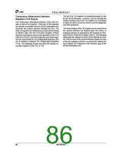
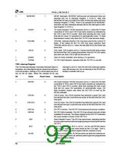
TIR0: Network Control
General control for the transceiver device attached to
the transceiver interface pins.
Bit
Name
Reset Value
Description
7
LNK
pin
Link LED. The inverse of the LNK bit value is driven onto the LNK
pin when the LNK pin has been enabled for output.
The value read from LNK will always represent the inversion of the
current value of the LNK pin. The control of the function of the LNK
pin is described in the Multi-Function Pin section.
6
ACT
pin
Activity LED. The inverse of the ACT bit value is driven onto the
ACT pin when the ACT pin has been enabled for output.
The value read from ACT will always represent the inversion of the
current value of the ACT pin. The control of the function of the ACT
pin is described in the Multi-Function Pin section.
5
4
SRES
0
0
TAI reset. Active high. Asserting this bit will reset the TAI portion of
the Am79C930 device, except for this register (i.e., TIR0).
SSTRB
Software Strobe. This bit is intended for software development use.
The value written to this bit will be sent to the test output when the
device is programmed for test mode.
3
2
Reserved
RXP
–
0
Reserved. Must be written as a 0. Reads of these bits produce
undefined data.
RX Power control. The inverse of the RXP bit value is driven onto
the RXPE pin when the RXPE pin has been enabled for output.
The value read from RXP will always represent the inverted logical
sense of the current value of the RXPE pin. The control of the func-
tion of the RXPE pin is described in the Multi-Function Pin section.
1
0
LFPE
HFPE
0
0
Low Frequency Power control. The inverse of the LFPE bit value is
driven onto the LFPE pin when the LFPE pin has been enabled
for output.
The value read from LFPE will always represent the inverted logical
sense of the current value of the LFPE pin. The control of the func-
tion of the LFPE pin is described in the Multi-Function Pin section.
High Frequency Power control. The inverse of the HFPE bit value is
driven onto the HFPE pin when the HFPE pin has been enabled
for output.
The value read from HFPE will always represent the inverted
logical sense of the current value of the HFPE pin. The control of
the function of the HFPE pin is described in the Multi-Function
Pin section.
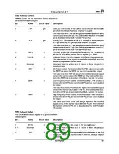
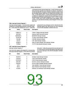
TIR1: Network Status
The TAI Network status register is a general network
status register.
Bit
Name
Reset Value
Description
7
TSTO
0
–
Test Output. This bit is the result of the test multiplexer.
6–3
Reserved
Reserved. Must be written as a 0. Reads of these bits produce
undefined data.
2
IRQ
0
Interrupt Request. This bit represents the current value of the IRQ
output pin. When IRQ has the value 1, then an interrupt request
is active.
Am79C930
89

 AMD [ AMD ]