AMD
P R E L I M I N A R Y
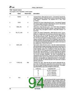
1
0
RXDRQ
TXDRQ
0
1
Receive FIFO DMA Request. This bit represents the current
value of the RXDRQ signal to the DRQ0 input of the 80188
embedded core.
Transmit FIFO DMA Request. This bit represents the current
value of the TXDRQ signal to the DRQ1 input of the 80188
embedded core.
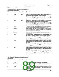
TIR2: Serial Device
TAI Serial Device register. This register is used to con-
trol the serial device interface.
Bit
Name
Reset Value
Description
7
Reserved
SDS[3:1]
–
Reserved. Must be written as a 0. Reads of this bit produce
undefined data.
6–4
000b
Serial Device Select. Each of these bits controls one of the Serial
Device Select outputs of the Am79C930. Bit values are inverted as
they appear at the pins. As an example, writing a 1 to the SDS[3] bit
will cause the SDSEL3 output to be driven to a 0.
The value read from SDS[x] will always represent the current value
of the SDSEL[x] pin without inversion. The control of the function of
the SDSEL[x] pins are found in the Multi-Function Pin section.
3
SDCP
0
Serial Device Clock Auto pulse generation. When set to a 1, this bit
causes the SDCLK pin to become active for the duration of the WR#
signal at the 80188 interface of the TAI whenever the internal
Am79C930 TAI chip select has been activated and the memory bus
address present is 00010b, with higher order bits of MA as DON’T
CARE (i.e., a WRITE to TIR2 is occurring). The value of the SDCLK
pin during this strobe period depends upon the setting of the SDC
bit. The SDC bit gives the “inactive” state of the SDCLK pin. If SDCP
is set to 1, then the SDCLK pin is complemented from its inactive
state while either the 80188 WR# signal is active with the TAI chip
select also active. When SDCP is set to 0, then the SDC bit has di-
rect control of the SDCLK pin.
The value of the SDC bit must not be changed when the SDCP bit is
set to a 1. To change the value of SDC, first set SDCP to a 0.
The complete control of the function of the SDCLK pin is described
in the Multi-Function Pin section.
2
SDC
0
Serial Device Clock. The SDC bit value is driven onto the SDCLK
pin when the SDCLK pin has been enabled for output.
The value of the SDC bit must not be changed when the SDCP bit is
set to a 1. To change the value of SDC, first set SDCP to a 0.
The value read from SDC will always represent the current value of
the SDCLK pin. The control of the function of the SDCLK pin is de-
scribed in the Multi-Function Pin section.
1
0
SDDT
SDD
0
0
Serial Device Data Tristate. When SDDT is set to 1, the SDDATA
pin of the Am79C930 device is tri-stated. When SDDT is set to 0,
the SDDATA pin is driven with the value of the SDD bit.
The complete control of the function of the SDDATA pin is de-
scribed in the Multi-Function Pin section.
Serial Device Data. The SDD bit value is driven onto the SDDATA
pin when the SDDATA pin has been enabled for output.
90
Am79C930

 AMD [ AMD ]