AMD
P R E L I M I N A R Y
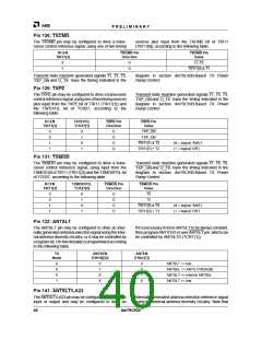
ENXCHBSY bit of TCR28 and the CHBSYU bit of
TIR5 and operates independently of the bits in the
table below.
This source of CCA information is controlled by the
ENXCHBSY bit of TCR28. When the ENXCHBSY bit of
TCR28 is set to
a 1, then the value of the
USER5/IRQ4/EXTCHBSY pin will be fed directly to the
CHBSYC bit of TIR4, CHBSY bit of TIR26 and the BCF
bit of TIR5. If the CHBSYC interrupt is unmasked, it will
produce an interrupt to the 80188 embedded controller.
If the BCF interrupt is unmasked, it will produce an inter-
rupttothe80188embeddedcontroller. Notethatsetting
the ENXCHBSY bit of TCR28 to a 1 will cause the
USER5/IRQ4/EXTCHBYS pin to function as an input,
regardless of the settings of the other control
bits listed.
In addition to the functionality listed above, the
USER5/IRQ4/EXTCHBSY pin may be used as the
source for CCA information, instead of relying on the in-
ternal CCA logic of the Am79C930 device. When using
the external CCA information, CCA information from the
internal logic will be unavailable. External CCA informa-
tion will appear in the same register bit locations as in-
ternal CCA information, when enabled, so a change
from internal source to external source will be transpar-
ent to firmware (excepting the necessary change in the
ENXCHBSY bit value).
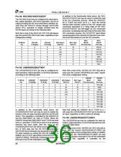
USER5/
IRQ4
Direction
USER5/
IRQ4
Pin Data
PCMCIA
Pin
ENXCHBSY
TCR28[5]
USER5FN
TCR7[5]
USER5EN
TCR15[2]
IRQ Select
PnPx70
IRQ Type
PnPx71
0
0
0
0
0
0
0
1
1
1
1
0
0
0
0
0
0
1
0
0
X
0
0
0
0
1
1
X
X
X
X
X
X
0
1
0
1
X
0
1
X
4h
4h
≠4h
≠4h
X
X
2h
1h
X
I
O
OD
I
TIR11[5]
IRQ4
IRQ4
TIR11[5]
TIR11[5]
TIR11[5]
TIR11[5]
TIR11[5]
TIR11[5]
TIR11[5]
X
O
I
X
X
X
O
I
X
X
X
X
I
X
X
O
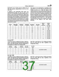
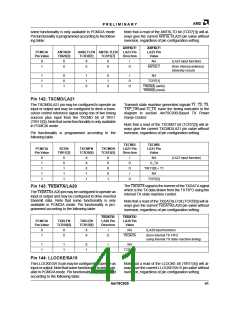
Pin 98: ACT
The ACT pin may be configured for input or output op-
eration. The output drive may be programmed for totem
pole or open drain operation. ACT pin configuration is
accomplished according to the following table:
Note that a read of the ACT bit (TIR0[6]) will always
give the current ACT pin value, regardless of pin
configuration setting.
ACTEN
TCR15[1]
ACT
TIR0[6]
ACTDR
TCR27[3]
ACT Pin
Direction
ACT Pin
Value
0
1
1
1
1
X
0
1
0
1
X
0
0
1
1
I
NA
OD
OD
O
float
LOW
HIGH
LOW
reset default condition
O
Pin 100: LNK
The LNK pin may be configured for input or output op-
eration. The output drive may be programmed for totem
pole or open drain operation. LNK pin configuration is
accomplished according to the following table:
Note that a read of the LNK bit (TIR0[7]) will always
give the current LNK pin value, regardless of pin
configuration setting.
LNKEN
LNK
LNKDR
LNK Pin
LNK Pin
TCR13[7]
TIR0[7]
TCR27[4]
Direction
Value
0
1
1
1
1
X
0
1
0
1
X
0
0
1
1
I
NA
OD
OD
O
float
LOW
HIGH
LOW
reset default condition
O
Am79C930
37

 AMD [ AMD ]