AMD
P R E L I M I N A R Y
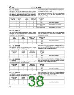
operation. SDCLKpinconfigurationisaccomplishedac-
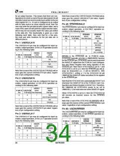
Pin 101: SDCLK
cording to the following table:
The SDCLK pin may be configured for input or output
operation. Theoutputdrivemaybeprogrammedforreg-
ister-driven or auto-pulse generation. The auto-pulse
may be programmed for either active low or active high
Note that a read of the SDC bit (TIR2[2]) will always
give the current SDCLK pin value, regardless of pin
configuration setting.
SDCLKEN
TCR13[4]
SDCP
TIR2[3]
SDC
TIR2[2]
SDCLK Pin
Direction
SDCLK Pin
Value
0
1
1
1
1
X
0
1
0
1
X
0
0
1
1
I
NA
O
O
O
O
LOW
reset default condition
HIGH active pulse
HIGH
(when write to TIR2 occurs)
LOW active pulse
(when write to TIR2 occurs)
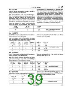
Pin 102: SDDATA
The SDDATA pin may be configured for input or output
operation. SDDATA pin configuration is accomplished
according to the following table:
Note that a read of the SDD bit (TIR2[0]) will always
give the current SDDATA pin value, regardless of pin
configuration setting.
SDDT
TIR2[1]
SDD
TIR2[0]
SDDATA Pin
Direction
SDDATA Pin
Value
0
0
1
0
1
X
O
O
I
LOW
HIGH
NA
reset default condition
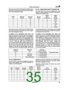
Note that a read of the SDS[3] bit (TIR2[6]) will always
give the current SDSEL[3] pin value without inversion,
regardless of pin configuration setting.
Pin 103: SDSEL3
The SDSEL[3] pin may be configured for input or output
operation according to the following table:
SDSEL3EN
SDS[3]
SDSEL[3]
SDSEL[3]
TCR13[3]
TIR2[6]
Pin Direction
Pin Value
0
1
1
X
0
1
I
NA
O
O
HIGH
LOW
reset default condition
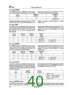
Note that a read of the SDS[2] bit (TIR2[5]) will always
give the current SDSEL[2] pin value without inversion,
regardless of pin configuration setting.
Pin 105: SDSEL2
The SDSEL[2] pin may be configured for input or output
operation according to the following table:
SDSEL2EN
SDS[2]
SDSEL[2]
SDSEL[2]
TCR13[2]
TIR2[5]
Pin Direction
Pin Value
0
1
1
X
0
1
I
NA
O
O
HIGH
LOW
reset default condition
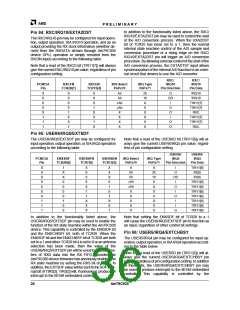
Note that a read of the SDS[1] bit (TIR2[4]) will always
give the current SDSEL[1] pin value without inversion,
regardless of pin configuration setting.
Pin 107: SDSEL1
The SDSEL[1] pin may be configured for input or output
operation according to the following table:
SDSEL1EN
TCR13[1]
SDS[1]
TIR2[4]
SDSEL[1]
Pin Direction
SDSEL[1]
Pin Value
0
1
1
X
0
1
I
NA
O
O
HIGH
LOW
reset default condition
38
Am79C930

 AMD [ AMD ]