AMD
P R E L I M I N A R Y
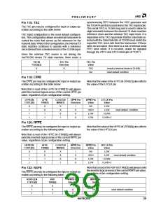
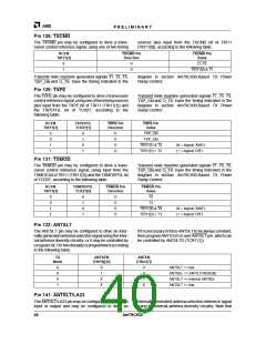
Pin 126: TXCMD
The TXCMD pin may be configured to drive a trans-
ceiver control reference signal, using one of two timing
sources plus input from the TXCMD bit of TIR11
(TIR11[0]), according to the following table:
RCEN
TIR11[3]
TXCMD Pin
Direction
TXCMD Pin
Value
0
1
O
O
O_TX
TIR11[0] & T1
Transmit state machine generated signals T1, T2, T3,
TXP_ON and O_TX have the timing indicated in the
diagram in section Am79C930-Based TX Power
Ramp Control.
Pin 129: TXPE
The TXPE pin may be configured to drive a transceiver
controlreferencesignal, usingoneoftwotimingsources
plus input from the TXPE bit of TIR11 (TIR11[1]) and
the TXPEPOL bit of TCR27, according to the
following table:
Transmit state machine generated signals T1, T2, T3,
TXP_ON and O_TX have the timing indicated in the
diagram in section Am79C930-Based TX Power
Ramp Control.
RCEN
TIR11[3]
TXPEPOL
TCR27[1]
TXPE Pin
Direction
TXPE Pin
Value
0
0
1
1
0
1
0
1
O
O
O
O
TXP_ON
TXP_ON
TIR11[1] & T2
(& = logical ‘AND’)
(+ = logical ‘OR’)
TIR11[1] + T2
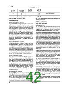
Pin 131: TXMOD
The TXMOD pin may be configured to drive a trans-
ceiver control reference signal, using input from the
TXMOD bit of TIR11 (TIR11[2]) and the TXMODPOL bit
of TCR27, according to the following table:
Transmit state machine generated signals T1, T2, T3,
TXP_ON and O_TX have the timing indicated in the
diagram in section Am79C930-Based TX Power
Ramp Control.
RCEN
TIR11[3]
TXMODPOL
TCR27[0]
TXMOD Pin
Direction
TXMOD Pin
Value
0
0
1
1
0
1
0
1
O
O
O
O
T3
T3
TIR11[2] & T3
(& = logical ‘AND’)
(+ = logical ‘OR’)
TIR11[2] + T3
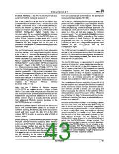
Pin 132: ANTSLT
The ANTSLT pin may be configured to drive an inter-
nally generated antenna selection signal using the inter-
nal antenna diversity circuitry, or it may be controlled by
a register bit. Pin functionality is programmed according
to the following table:
If it is necessary to force ANTSLT to be always constant,
then program ANTS to 0 or userANTSLT pin, which can
be controlled by ANTSLTD (TCR7:[1]).
TX
ANTSEN
ANTEN
Mode
(TIR16[[3])
(TIR4:[7])
0
0
0
1
0
1
0
0
1
X
ANTSLT <= low
ANTSEL <= ANTS (TIR26:[4])
ANTSLT <= internal ANTSEL
ANTSLT <= low
X
X
Pin 141: ANTSLT/LA23
The ANTSLT/LA23 pin may be configured to operate as
input or output and may be configured to drive an
internally generated antenna selection reference signal
using the internal antenna diversity circuitry. Note that
40
Am79C930

 AMD [ AMD ]