AMD
P R E L I M I N A R Y
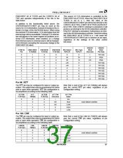
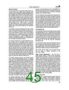
some functionality is only available in PCMCIA mode.
Pin functionality is programmed according to the follow-
ing table:
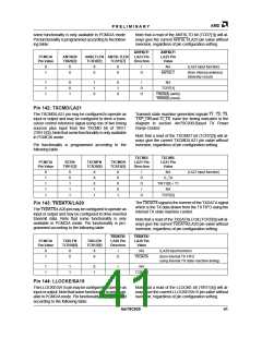
Note that a read of the ANTSLTD bit (TCR7[1]) will al-
ways give the current ANTSLT/LA23 pin value without
inversion, regardless of pin configuration setting.
ANTSLT/
LA23 Pin
Direction
ANTSLT/
LA23 Pin
Value
PCMCIA
Pin Value
ANTSEN
TIR26[3]
ANSLTLFN ANTSLTLEN
TCR30[7]
TCR15[7]
0
1
X
0
X
0
X
X
I
NA
(LA23 input function)
O
ANTSLT
(from internal antenna)
(diversity circuit)
1
1
1
X
X
1
1
1
0
0
1
X
I
NA
O
O
TCR7[1]
TIR26[4] (write)
TIR26[5] (read)
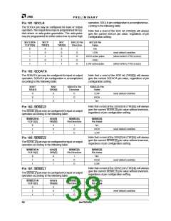
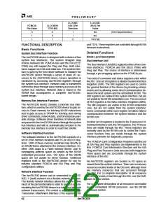
Pin 142: TXCMD/LA21
The TXCMD/LA21 pin may be configured to operate as
input or output and may be configured to drive a trans-
ceiver control reference signal using one of two timing
sources plus input from the TXCMD bit of TIR11
(TIR11[0]). Note that some functionality is only available
in PCMCIA mode.
Transmit state machine generated signals T1, T2, T3,
TXP_ON and O_TX have the timing indicated in the
diagram in section Am79C930-Based TX Power
Ramp Control.
Note that a read of the TXCMDT bit (TCR7[2]) will al-
ways give the current TXCMD/LA21 pin value without
inversion, regardless of pin configuration setting.
Pin functionality is programmed according to the
following table.
TXCMD/
LA21 Pin
Direction
TXCMD/
LA21 Pin
Value
PCMCIA
Pin Value
RCEN
TIR11[3]
TXCMFN
TCR30[5]
TXCMEN
TCR15[5]
0
1
1
1
1
X
0
1
1
1
X
X
0
1
1
X
X
X
0
I
NA
O_TX
(LA21 input function)
O
O
I
TIR11[0] + T1
NA
1
O
TCR7[2]
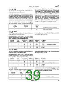
The TXDATA signal is the inverse of the TXDATA signal
which is the TX data drawn from the TX FIFO using the
internal TX state machine control.
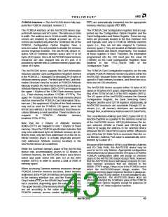
Pin 143: TXDATA/LA20
The TXDATA/LA20 pin may be configured to operate as
input or output and may be configured to drive inverted
transmit data. Note that some functionality is only
available in PCMCIA mode. Pin functionality is pro-
grammed according to the following table:
Note that a read of the TXDATALD bit (TCR7[0]) will al-
ways give the current TXDATA/LA20 pin value without
inversion, regardless of pin configuration setting.
TXDATA/
LA20 Pin
Direction
TXDATA/
LA20 Pin
Value
PCMCIA
Pin Value
TXDLFN
TCR30[6]
TXDLEN
TCR15[6]
0
1
X
0
X
X
I
NA
(LA20 input function)
O
TXDATA
(from internal TX FIFO
using internal TX state machine timing)
1
1
1
1
0
1
I
NA
O
TCR7[0]
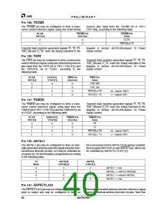
Pin 144: LLOCKE/SA15
The LLOCKE/SA15 pin may be configured to operate as
inputoroutput. Notethatsomefunctionalityisonlyavail-
able in PCMCIA mode. Pin functionality is programmed
according to the following table:
Note that a read of the LLOCKE bit (TIR11[4]) will al-
ways give the current LLOCKE/SA15 pin value without
inversion, regardless of pin configuration setting.
Am79C930
41

 AMD [ AMD ]