P R E L I M I N A R Y
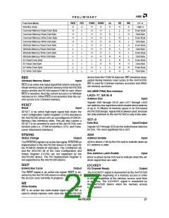
ISA PLUG AND PLAY PIN SUMMARY
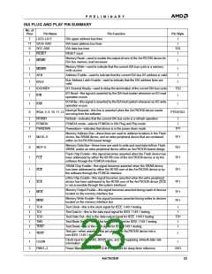
No. of
Pins
Pin Name
LA23–LA17
Pin Function
Pin Style
7
17
8
ISA upper address bus lines
ISA lower address bus lines
ISA data bus lines
I
SA16–SA0
SD7–SD0
RESET
I
TS2
I
1
RESET input
Memory Read—used to enable the output drivers of the Am79C930 device for
ISA bus memory read accesses
1
MEMR
I
Memory Write—used to indicate that the current ISA bus cycle is a memory
write access
1
1
1
1
1
MEMW
AEN
I
Address Enable—used to indicate that the current ISA bus I/O address is valid
I
Bus Address Latch Enable—used to indicate that the ISA address lines are
valid
BALE
I
IOCHRDY
IOR
I/O Channel Ready—used to delay the termination of the current ISA bus cycle
TS2
I
I/O Read—this signal is asserted by the ISA host system whenever an I/O read
operation occurs
I/O Write—this signal is asserted by the ISA host system whenever an I/O write
operation occurs
1
6
IOW
I
Interrupt Request—this line is asserted when the Am79C930 device needs
servicing from the software
IRQ4, 5, 9, 10, 11, 12
PTS3/OD2
1
1
1
RFRSH
Refresh—indicates that the current ISA bus cycle is a refresh operation
PCMCIA mode—selects PCMCIA or ISA Plug and Play mode
Powerdown—indicates that device is in the power down mode
I
I
PCMCIA
PWRDWN
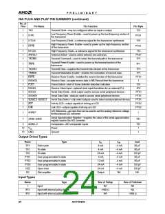
TP1
Memory Address Bus—these lines are used to address locations in the Flash
device, the SRAM device, and an extra peripheral device that are contained
within an Am79C930-based design
17
8
MA16–0
MD7–0
FCE
TP1
TS1
TP1
Memory Data Bus—these lines are used to write and read data to/from Flash,
SRAM, and/or an extra peripheral device within an Am79C930-based design
Flash Chip Enable—this signal becomes asserted when the Flash device has
been addressed by either the 80188 core of the Am79C930 device or by the
software through the PCMCIA interface
1
SRAM Chip Enable—this signal becomes asserted when the SRAM device
has been addressed by either the 80188 core of the Am79C930 device or by
the software through the PCMCIA interface
1
1
SCE
XCE
TP1
TP1
eXtra Chip Enable—this signal becomes asserted when the extra peripheral
device has been addressed by the 80188 core of the Am79C930 device (XCE
is not accessible through the system interface)
Memory Output Enable—this signal becomes asserted during reads of devices
located on the memory interface bus
1
1
MOE
MWE
TP1
TP1
Memory Write Enable—this signal becomes asserted during writes to devices
located on the memory interface bus
1
1
1
1
1
TCK
TDI
Test Clock—this is the clock signal for IEEE 1149.1 testing
Test Data In—this is the data input signal for IEEE 1149.1 testing
Test Data Out—this is the data output signal for IEEE 1149.1 testing
Test Mode Select—this is the test mode select for IEEE 1149.1 testing
Test Reset—this is the reset signal for IEEE 1149.1 testing
I
I
TDO
TMS
TRST
TS1
I
I
Test pin—when asserted, this pin places the Am79C930 device into a
non-IEEE 1149.1 test mode
1
TEST
I
Clock input to drive BIU, 80188 core, and TAI, supplying network data rate
information
1
2
CLKIN
I
PMX1–2
Power Management Xtal—32-kHz Xtal input for sleep timer reference
I/XO
Am79C930
23

 AMD [ AMD ]