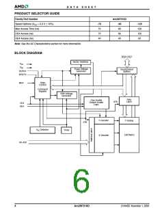
D A T A S H E E T
DEVICE BUS OPERATIONS
This section describes the requirements and use of the
device bus operations, which are initiated through the
internal command register. The command register it-
self does not occupy any addressable memory
location. The register is composed of latches that store
the commands, along with the address and data infor-
mation needed to execute the command. The contents
of the register serve as inputs to the internal state ma-
chine. The state machine outputs dictate the function of
the device. The appropriate device bus operations
table lists the inputs and control levels required, and the
resulting output. The following subsections describe
each of these operations in further detail.
Table 1. Am29F016D Device Bus Operations
Operation
CE#
OE#
L
WE#
H
RESET#
A0–A20
DQ0–DQ7
DOUT
Read
Write
L
H
AIN
AIN
X
L
H
L
H
DIN
CMOS Standby
TTL Standby
VCC 0.5 V
X
X
VCC 0.5 V
High-Z
High-Z
High-Z
High-Z
H
L
X
X
H
H
L
X
Output Disable
Hardware Reset
H
H
X
X
X
X
X
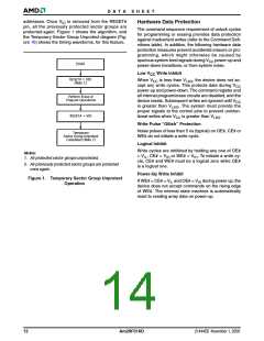
Temporary Sector Unprotect
(See Note)
X
X
X
VID
AIN
DIN
Legend:
L = Logic Low = VIL, H = Logic High = VIH, VID = 12.0 ± 0.5 V, X = Don’t Care, DIN = Data In, DOUT = Data Out, AIN = Address In
Note: See the sections on Sector Group Protection and Temporary Sector Unprotect for more information
Requirements for Reading Array Data
Writing Commands/Command Sequences
To read array data from the outputs, the system must
To write a command or command sequence (which in-
cludes programming data to the device and erasing
sectors of memory), the system must drive WE# and
drive the CE# and OE# pins to V . CE# is the power
IL
control and selects the device. OE# is the output control
and gates array data to the output pins. WE# should re-
CE# to V , and OE# to V .
IL
IH
main at V .
IH
An erase operation can erase one sector, multiple sec-
tors, or the entire device. The Sector Address Tables
indicate the address space that each sector occupies.
A “sector address” consists of the address bits required
to uniquely select a sector. See the “Command Defini-
tions” section for details on erasing a sector or the
entire chip, or suspending/resuming the erase
operation.
The internal state machine is set for reading array
data upon device power-up, or after a hardware reset.
This ensures that no spurious alteration of the mem-
ory content occurs during the power transition. No
command is necessary in this mode to obtain array
data. Standard microprocessor read cycles that as-
sert valid addresses on the device address inputs
produce valid data on the device data outputs. The
device remains enabled for read access until the
command register contents are altered.
After the system writes the autoselect command se-
quence, the device enters the autoselect mode. The
system can then read autoselect codes from the inter-
nal register (which is separate from the memory array)
on DQ7–DQ0. Standard read cycle timings apply in this
mode. Refer to the “Autoselect Mode” and “Autoselect
Command Sequence” sections for more information.
See “Reading Array Data” for more information. Refer
to the AC Read Operations table for timing specifica-
tions and to the Read Operations Timings diagram for
the timing waveforms. I
in the DC Characteristics
CC1
table represents the active current specification for
reading array data.
I
in the DC Characteristics table represents the ac-
CC2
tive current specification for the write mode. The “AC
Characteristics” section contains timing specification
tables and timing diagrams for write operations.
8
Am29F016D
21444E6 November 1, 2006

 AMD [ AMD ]