Revision 1.02 – April 12, 2007
S5920 – PCI Product: Pass-Thru Operation
Data Book
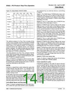
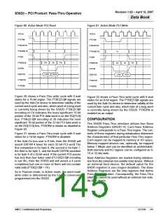
Clock 2: Since this region does have PTADR#
enabled as an output, it is driven active (low) and the
PCI address for the current transaction is presented
on the DQ[31:0] bus.
Clock 11: The final data word (DATA4) must be
latched by the Add-On device at the rising edge of this
clock. PTBE# is driven to Fh indicating all 4 bytes have
been accessed. PTNUM and PTWR may change state
since the access is complete.
Clock 3: The Add-On device must latch the PCI
address at the rising edge of this clock.
Clock 12: PTBE# may change state.
Clock 4: DXFR# is asserted low indicating that data
will be transferred on the next rising clock edge (clock
5). Data1 is driven onto the DQ[31:0] bus.
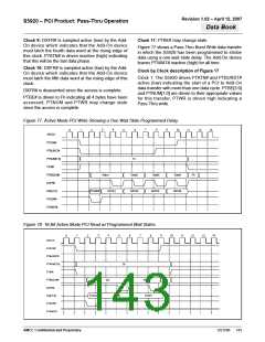
Active Mode with 16/8-bit data buses
When the S5920 is programmed in Active mode and
16-bit, the DXFR# output will strobe twice for every
PCI 32-bit word that has been read/written. Each
DXFR# assertion signifies that a 16-bit word has been
transferred to the Add-On side. The first DXFR# com-
pletion will be for the least significant 16-bit word of a
32-bit word (“LOW” in Figures 18, 9-20 and 9-21),
while the second transfer will be for the most signifi-
cant 16-bit word (“HIGH” in Figures 18, 9-20 and 9-
21). If the current PCI access has only 2 bytes valid
(PCI BE[3:0]# encoding of Ch or 3h instead of 0h),
then the S5920 will still assert a 2 cycle completion but
one of them will not contain valid data
(PTBE[3:0]#=Fh). If the programmed wait states for
the current Pass-Thru region is not zero, then the
S5920 will insert the programmed wait states before
the “LOW” data word and also between the “LOW” and
“HIGH” data words. Figure 18 shows a PCI read to a
16-bit Add-On region with two programmed wait
states. Note that a PCI read to an 8-bit Add-On would
be the same as Figure 18 except that there would be 4
data transfers (one for each byte) vice 2.
Clock 5: The Add-On device must latch the first data
word at the rising edge of this clock. Valid data is
determined by decoding the PTBE[3:0]# lines.
Clock 6: DXFR# is asserted indicating that data will be
transferred on the next rising clock edge (clock 7).
DATA2 is driven onto the DQ[31:0] bus.
Clock 7: The Add-On side device latches the second
data word (DATA2) at the rising edge of this clock.
Clock 8: DXFR# is asserted indicating that data will be
transferred on the next rising clock edge (clock 9).
DATA3 is driven onto the DQ[31:0] bus. PTBURST# is
driven inactive indicating that after this data word is
transferred, there is only one data word left to transfer.
Clock 9: The Add-On side device latches the third
data word (DATA3) at this clock edge.
Clock 10: DXFR# is asserted indicating that data will
be transferred on the next rising clock edge (clock 11).
DATA4 is driven onto the DQ[31:0] bus. PTATN# is
deasserted indicating that this will be the last data
phase.
As in Passive mode, in Active mode, the word read/
write order is determined by the Endian conversion
programmed into the S5920.
Figure 79. Active Mode PCI Read w/ Programmed Wait States
3
4
9
14
0
1
2
5
6
7
8
10
11
12
13
ADCLK
PTATN#
PTBURST#
PTNUM[1:0]
PTWR
1h
PTBE[3:0]#
DXFR#
Fh
Data1
Data2
Data3
DQ[31:0]
PTADR#
PTWAIT#
PTADDR
DATA1
DATA2
DATA3
AMCC Confidential and Proprietary
DS1596
144

 AMCC [ APPLIED MICRO CIRCUITS CORPORATION ]