QUAD GIGABIT ETHERNET TRANSCEIVER
S2066
The S2066 synthesizes a serial transmit clock from
the reference signal provided. The S2066 will obtain
phase and frequency lock within 2500 bit times after
the start of receiving reference clock inputs. Reliable
locking of the transmit PLL is assured, but a lock-
detect output is NOT provided.
The frequency of the reference clock must be either
1/10 the serial data rate, CLKSEL = 0, or 1/20 the
serial data rate, CLKSEL = 1. Note that in both
cases, the frequency of the parallel word rate output,
TCLKO, is constant at 1/10 the serial data rate.
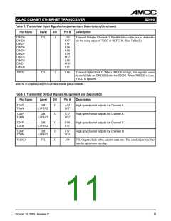
Serial Data Outputs
Test Functions
The S2066 provides LVPECL level serial outputs.
Each high speed output should be provided with a
resistor to VSS (Gnd) near the device. A value of
4.5KΩ provides optimal performance with minimum
impact on power dissipation. The resistance may be
as low as 450Ω, but will dissipate additional power
with no substantive performance improvement.
The S2066 can be configured for factory test to aid
in functional testing of the device. When in the test
mode, the internal transmit and receive voltage-con-
trolled oscillator (VCO) is bypassed and the refer-
ence clock substituted. This allows full functional
testing of the digital portion of the chip or bypassing
the internal synthesized clock with an external clock
source. (See the section Other Operating Modes.)
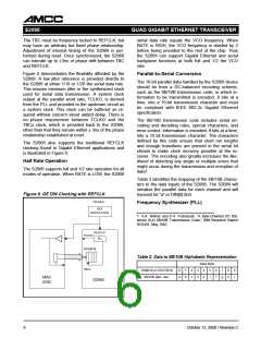
Transmit FIFO Initialization
The transmit FIFO must be initialized after stable
delivery of data and TBC to the parallel interface,
and before entering the normal operational state of
the circuit. FIFO initialization is performed upon the
de-assertion of the RESET signal. The DIN FIFO is
automatically reset upon power up immediately after
the DIN PLL obtains stable frequency lock. If the
circuit has not reached steady state timing at this
point, then the user must initialize by asserting the
RESET signal. The TCLKO output will operate nor-
mally even when RESET is asserted and is available
for use as an upstream clock source.
Reference Clock Input
The reference clock input must be supplied with a
low-jitter clock source. All reference clocks in a sys-
tem must be within 200 ppm of each other to insure
that the clock recovery units can lock to the serial
data.
7
October 13, 2000 / Revision C

 AMCC [ APPLIED MICRO CIRCUITS CORPORATION ]