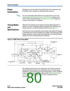
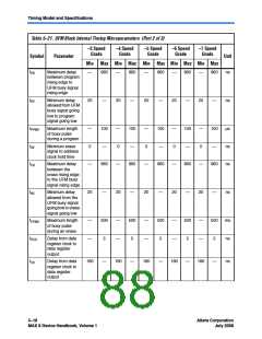
Timing Model and Specifications
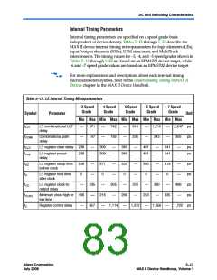
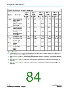
Table 5–16. IOE Internal Timing Microparameters
–3 Speed
Grade
–4 Speed
Grade
–5 Speed
Grade
–6 Speed
Grade
–7 Speed
Grade
Symbol
Parameter
Unit
Min Max Min Max Min Max Min Max Min Max
tFASTIO
Data output delay
fromadjacentLEto
I/O block
—
159
—
207
—
254
—
170
—
348
970
ps
tIN
I/O input pad and
buffer delay
—
—
708
—
—
920
—
—
1,132
2,430
—
—
907
—
—
ps
tGLOB (1) I/O input pad and
buffer delay used
1,519
1,974
2,261
2,670 ps
as global signal pin
tIOE
Internally
generated output
enable delay
—
354
—
374
—
460
—
530
—
966
410
ps
ps
tDL
Input routing delay
—
—
224
—
—
291
—
—
358
—
—
318
—
—
tOD (2)
Output delay buffer
and pad delay
1,064
1,383
1,702
1,319
1,526 ps
tXZ (3)
tZX (4)
Output buffer
disable
delay
—
—
756
—
—
982
—
—
1,209
1,604
—
—
1,045
1,160
—
—
1,264 ps
Output buffer
enable
1,003
1,303
1,325 ps
delay
Notes to Table 5–16:
(1) Delay numbers for tGLOB differ for each device density and speed grade. The delay numbers for tGLOB, shown in
Table 5–16, are based on an EPM240 device target.
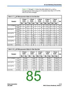
(2) Refer to Tables 5–29 and 5–31 for delay adders associated with different I/O standards, drive strengths, and slew
rates.
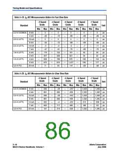
(3) Refer to Tables 5–19 and 5–20 for tXZ delay adders associated with different I/O standards, drive strengths, and
slew rates.
(4) Refer to Tables 5–17 and 5–18 for tZX delay adders associated with different I/O standards, drive strengths, and
slew rates.
5–14Core Version a.b.c variable
MAX II Device Handbook, Volume 1
Altera Corporation
July 2008

 ALTERA [ ALTERA CORPORATION ]