Power Consumption
Designers can use the Altera® PowerPlay Early Power Estimator and
PowerPlay Power Analyzer to estimate the device power.
Power
Consumption
f
For more information about these power analysis tools, refer to the
Understanding and Evaluating Power in MAX II Devices chapter in the
MAX II Device Handbook and the PowerPlay Power Analysis chapter in
volume 3 of the Quartus II Handbook.
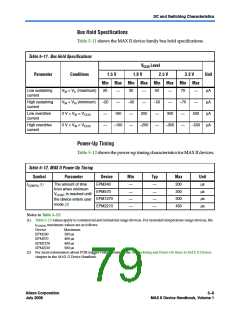
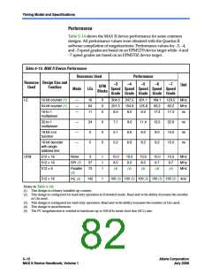
MAX II devices timing can be analyzed with the Altera Quartus® II
software, a variety of popular industry-standard EDA simulators and
timing analyzers, or with the timing model shown in Figure 5–2.
Timing Model
and
Specifications
MAX II devices have predictable internal delays that enable the designer
to determine the worst-case timing of any design. The software provides
timing simulation, point-to-point delay prediction, and detailed timing
analysis for device-wide performance evaluation.
Figure 5–2. MAX II Device Timing Model
Output and Output Enable
Data Delay
tR4
tIODR
tIOE
Data-In/LUT Chain
Output Routing
Delay
User
Flash
Memory
Logic Element
LUT Delay
Output
Delay
tOD
tXZ
tZX
tC4
tLUT
tCOMB
tFASTIO
tCO
tSU
tH
tPRE
tCLR
Input Routing
Delay
I/O Input Delay
Register Control
Delay
I/O Pin
tIN
tDL
tC
From Adjacent LE
tGLOB
INPUT
Combinational Path Delay
I/O Pin
Global Input Delay
To Adjacent LE
Register Delays
Data-Out
The timing characteristics of any signal path can be derived from the
timing model and parameters of a particular device. External timing
parameters, which represent pin-to-pin timing delays, can be calculated
as the sum of internal parameters. Refer to the Understanding Timing in
MAX II Devices chapter in the MAX II Device Handbook for more
information.
5–10Core Version a.b.c variable
MAX II Device Handbook, Volume 1
Altera Corporation
July 2008

 ALTERA [ ALTERA CORPORATION ]