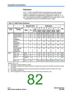
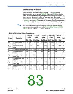
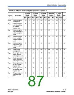
DC and Switching Characteristics
Internal Timing Parameters
Internal timing parameters are specified on a speed grade basis
independent of device density. Tables 5–15 through 5–22 describe the
MAX II device internal timing microparameters for logic elements (LEs),
input/output elements (IOEs), UFM structures, and MultiTrack
interconnects. The timing values for –3, –4, and –5 speed grades shown in
Tables 5–15 through 5–22 are based on an EPM1270 device target, while
–6 and –7 speed grade values are based on an EPM570Z device target.
f
For more explanations and descriptions about each internal timing
microparameters symbol, refer to the Understanding Timing in MAX II
Devices chapter in the MAX II Device Handbook.
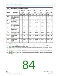
Table 5–15. LE Internal Timing Microparameters
–3 Speed
Grade
–4 Speed
Grade
–5 Speed
Grade
–6 Speed
Grade
–7 Speed
Grade
Symbol
Parameter
Unit
Min Max Min Max Min Max Min Max Min Max
tLUT
LE combinational LUT
delay
—
571
—
742
—
914
—
1,215
—
2,247 ps
tCOMB
Combinational path
delay
—
147
—
192
—
236
—
243
—
305
ps
tCLR
tPRE
LE register clear delay 238
—
—
309
309
—
—
381
381
—
—
401
401
—
—
541
541
—
—
ps
ps
LE register preset
delay
238
208
0
tSU
tH
LE register setup time
before clock
—
—
271
0
—
—
333
0
—
—
260
0
—
—
319
0
—
—
ps
ps
ps
ps
LE register hold time
after clock
tCO
tCLKHL
tC
LE register clock-to-
output delay
—
235
—
305
—
—
376
—
—
380
—
—
489
—
Minimum clock high or 166
low time
216
—
266
—
253
—
335
—
—
Register control delay
—
857
1,114
1,372
1,356
1,722 ps
Altera Corporation
July 2008
5–13
MAX II Device Handbook, Volume 1

 ALTERA [ ALTERA CORPORATION ]