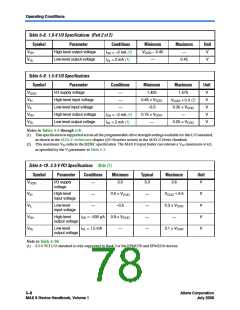
Operating Conditions
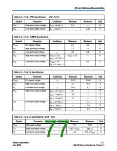
Table 5–8. 1.8-V I/O Specifications (Part 2 of 2)
Symbol
Parameter
Conditions
Minimum
VCCIO – 0.45
—
Maximum
Unit
V
VOH
VOL
High-level output voltage
Low-level output voltage
I
OH = –2 mA (1)
—
0.45
V
IOL = 2 mA (1)
Table 5–9. 1.5-V I/O Specifications
Symbol
Parameter
Conditions
Minimum
1.425
Maximum
1.575
Unit
V
VCCIO
I/O supply voltage
—
—
VIH
VIL
High-level input voltage
Low-level input voltage
High-level output voltage
Low-level output voltage
0.65 × VCCIO
–0.3
V
VCCIO + 0.3 (2)
0.35 × VCCIO
—
V
—
VOH
VOL
0.75 × VCCIO
—
V
IOH = –2 mA (1)
IOL = 2 mA (1)
0.25 × VCCIO
V
Notes to Tables 5–5 through 5–9:
(1) This specification is supported across all the programmable drive strength settings available for this I/O standard,
as shown in the MAX II Architecture chapter (I/O Structure section) in the MAX II Device Handbook.
(2) This maximum VIH reflects the JEDEC specification. The MAX II input buffer can tolerate a VIH maximum of 4.0,
as specified by the VI parameter in Table 5–2.
Table 5–10. 3.3-V PCI Specifications Note (1)
Symbol
Parameter
Conditions
Minimum
Typical
Maximum
Unit
VCCIO
I/O supply
voltage
3.0
3.3
3.6
V
—
VIH
VIL
High-level
input voltage
0.5 × VCCIO
–0.5
VCCIO + 0.5
0.3 × VCCIO
V
V
V
V
—
—
—
—
—
Low-level
input voltage
—
VOH
VOL
High-level
output voltage
IOH = –500 µA
IOL = 1.5 mA
0.9 × VCCIO
—
—
Low-level
0.1 × VCCIO
output voltage
Note to Table 5–10:
(1) 3.3-V PCI I/O standard is only supported in Bank 3 of the EPM1270 and EPM2210 devices.
5–8Core Version a.b.c variable
MAX II Device Handbook, Volume 1
Altera Corporation
July 2008

 ALTERA [ ALTERA CORPORATION ]