DC and Switching Characteristics
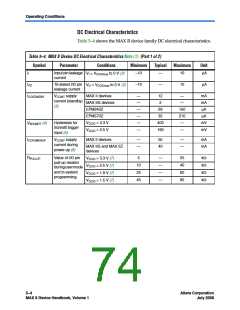
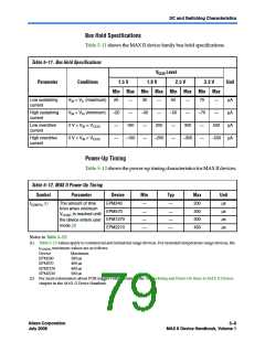
Table 5–4. MAX II Device DC Electrical Characteristics Note (1) (Part 2 of 2)
Symbol
Parameter
Conditions
Minimum
Typical
Maximum
Unit
IPULLUP
I/O pin pull-up
resistor current
when I/O is
—
—
—
300
µA
unprogrammed
CIO
Input
capacitance for
user I/O pin
—
—
—
—
—
—
8
8
pF
pF
CGCLK
Input
capacitance for
dual-purpose
GCLK/user I/O
pin
Notes to Table 5–4:
(1) Typical values are for TA = 25 °C, VCCINT = 3.3 or 2.5 V, and VCCIO = 1.5 V, 1.8 V, 2.5 V, or 3.3 V.
(2) This value is specified for normal device operation. The value may vary during power-up. This applies for all VCCIO
settings (3.3, 2.5, 1.8, and 1.5 V).
(3) VI = ground, no load, no toggling inputs.
(4) This value applies to commercial and industrial range devices. For extended temperature range devices, the
VSCHMITT typical value is 300 mV for VCCIO = 3.3 V and 120 mV for VCCIO = 2.5 V.
(5) The TCK input is susceptible to high pulse glitches when the input signal fall time is greater than 200 ns for all I/O
standards.
(6) This is a peak current value with a maximum duration of tCONFIG time.
(7) Pin pull-up resistance values will lower if an external source drives the pin higher than VCCIO
.
Altera Corporation
July 2008
5–5
MAX II Device Handbook, Volume 1

 ALTERA [ ALTERA CORPORATION ]