Hot Socketing and Power-On Reset in MAX II Devices
The DC specification applies when all VCC supplies to the device are
stable in the powered-up or powered-down conditions.
The hot socketing feature turns off (tri-states) the output buffer during the
power-up event (either VCCINT or VCCIO supplies) or power-down event.
The hot-socket circuit generates an internal HOTSCKTsignal when either
VCCINT or VCCIO is below the threshold voltage during power-up or
power-down. The HOTSCKTsignal cuts off the output buffer to make sure
that no DC current (except for weak pull-up leaking) leaks through the
pin. When VCC ramps up very slowly during power-up, VCC may still be
relatively low even after the power-on reset (POR) signal is released and
device configuration is complete.
Hot Socketing
Feature
Implementation
in MAX II
Devices
1
Make sure that the VCCINT is within the recommended operating
range even though SRAM download has completed.
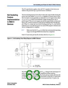
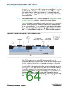
Each I/O and clock pin has the circuitry shown in Figure 4–1.
Figure 4–1. Hot Socketing Circuit Block Diagram for MAX II Devices
Power On
Reset
Monitor
VCCIO
Weak
Pull-Up
Resistor
Output Enable
PAD
Voltage
Tolerance
Control
Hot Socket
Input Buffer
to Logic Array
The POR circuit monitors VCCINT and VCCIO voltage levels and keeps I/O
pins tri-stated until the device has completed its flash memory
configuration of the SRAM logic. The weak pull-up resistor (R) from the
I/O pin to VCCIO is enabled during download to keep the I/O pins from
floating. The 3.3-V tolerance control circuit permits the I/O pins to be
Altera Corporation
December 2007
4–3
MAX II Device Handbook, Volume 1

 ALTERA [ ALTERA CORPORATION ]