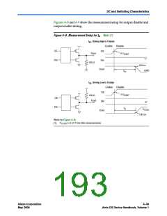
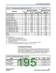
I/O Timing Model
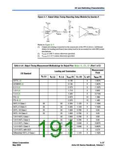
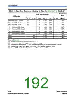
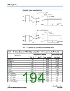
Table 4–44. Output Timing Measurement Methodology for Output Pins Notes (1), (2), (3) (Part 2 of 2)
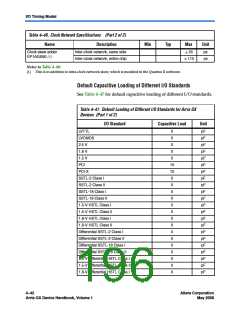
Measurement
Loading and Termination
RD (Ω) RT (Ω) VCCIO (V) VTT (V) CL (pF)
Point
I/O Standard
RS (Ω)
VMEAS (V)
Differential SSTL-2 Class II
Differential SSTL-18 Class I
Differential SSTL-18 Class II
1.5-V differential HSTL Class I
1.5-V differential HSTL Class II
1.8-V differential HSTL Class I
1.8-V differential HSTL Class II
LVDS
25
50
25
25
50
25
50
25
50
25
2.325
1.660
1.660
1.375
1.375
1.660
1.660
2.325
3.135
1.123
0.790
0.790
0.648
0.648
0.790
0.790
0
0
0
0
0
0
0
0
0
1.1625
0.83
0.83
0.6875
0.6875
0.83
0.83
100
100
1.1625
1.5675
LVPECL
Notes to Table 4–44:
(1) Input measurement point at internal node is 0.5 VCCINT
.
(2) Output measuring point for VMEAS at buffer output is 0.5 VCCIO
.
(3) Input stimulus edge rate is 0 to VCC in 0.2 ns (internal signal) from the driver preceding the I/O buffer.
(4) Less than 50-mV ripple on VCCIO and VCCPD, VCCINT = 1.15 V with less than 30-mV ripple.
(5) VCCPD = 2.97 V, less than 50-mV ripple on VCCIO and VCCPD, VCCINT = 1.15 V.
4–38
Altera Corporation
May 2008
Arria GX Device Handbook, Volume 1

 ALTERA [ ALTERA CORPORATION ]