DC and Switching Characteristics
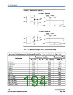
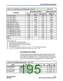
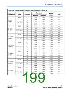
Table 4–45. Timing Measurement Methodology for Input Pins Notes (1), (2), (3), (4) (Part 2 of 2)
Measurement Conditions
Measurement Point
VMEAS (V)
I/O Standard
V
CCIO (V)
VREF (V)
Edge Rate (ns)
1.8-V HSTL Class II
1.660
1.375
1.375
1.140
2.325
2.325
1.660
1.660
1.375
1.375
1.660
1.660
2.325
3.135
0.830
0.688
0.688
0.570
1.163
1.163
0.830
0.830
0.688
0.688
0.830
0.830
1.660
1.375
1.375
1.140
2.325
2.325
1.660
1.660
1.375
1.375
1.660
1.660
0.100
0.100
0.83
0.6875
0.6875
0.570
1.1625
1.1625
0.83
1.5-V HSTL Class I
1.5-V HSTL Class II
1.2-V HSTL with OCT
Differential SSTL-2 Class I
Differential SSTL-2 Class II
Differential SSTL-18 Class I
Differential SSTL-18 Class II
1.5-V differential HSTL Class I
1.5-V differential HSTL Class II
1.8-V differential HSTL Class I
1.8-V differential HSTL Class II
LVDS
0.83
0.6875
0.6875
0.83
0.83
1.1625
1.5675
LVPECL
Notes to Table 4–45:
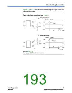
(1) Input buffer sees no load at buffer input.
(2) Input measuring point at buffer input is 0.5 VCCIO
.
(3) Output measuring point is 0.5 VCC at internal node.
(4) Input edge rate is 1 V/ns.
(5) Less than 50-mV ripple on VCCIO and VCCPD, VCCINT = 1.15 V with less than 30-mV ripple.
(6) VCCPD = 2.97 V, less than 50-mV ripple on VCCIO and VCCPD, VCCINT = 1.15 V.
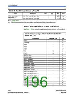
Clock Network Skew Adders
The Quartus II software models skew within dedicated clock networks
such as global and regional clocks. Therefore, the intra-clock network
skew adder is not specified. Table 4–46 specifies the clock skew between
any two clock networks driving registers in the I/O element (IOE).
Table 4–46. Clock Network Specifications (Part 1 of 2)
Name
Description
Min
Typ
Max
Unit
Clock skew adder
EP1AGX20/35 (1)
Inter-clock network, same side
Inter-clock network, entire chip
Inter-clock network, same side
Inter-clock network, entire chip
50
ps
ps
ps
ps
100
Clock skew adder
EP1AGX50/60 (1)
50
100
Altera Corporation
May 2008
4–41
Arria GX Device Handbook, Volume 1

 ALTERA [ ALTERA CORPORATION ]