I/O Timing Model
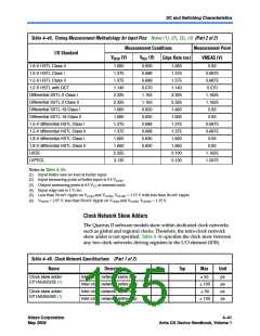
Table 4–46. Clock Network Specifications (Part 2 of 2)
Name
Description
Min
Typ
Max
Unit
Clock skew adder
EP1AGX90 (1)
Inter-clock network, same side
Inter-clock network, entire chip
55
ps
ps
110
Notes to Table 4–46:
(1) This is in addition to intra-clock network skew, which is modeled in the Quartus II software.
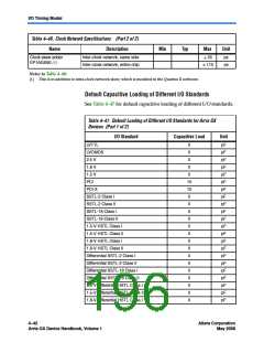
Default Capacitive Loading of Different I/O Standards
See Table 4–47 for default capacitive loading of different I/O standards.
Table 4–47. Default Loading of Different I/O Standards for Arria GX
Devices (Part 1 of 2)
I/O Standard
Capacitive Load
Unit
LVTTL
LVCMOS
2.5 V
0
0
pF
pF
pF
pF
pF
pF
pF
pF
pF
pF
pF
pF
pF
pF
pF
pF
pF
pF
pF
pF
pF
pF
0
1.8 V
0
1.5 V
0
PCI
10
10
0
PCI-X
SSTL-2 Class I
SSTL-2 Class II
0
SSTL-18 Class I
0
SSTL-18 Class II
0
1.5-V HSTL Class I
0
1.5-V HSTL Class II
0
1.8-V HSTL Class I
0
1.8-V HSTL Class II
0
Differential SSTL-2 Class I
Differential SSTL-2 Class II
Differential SSTL-18 Class I
Differential SSTL-18 Class II
1.5-V differential HSTL Class I
1.5-V differential HSTL Class II
1.8-V differential HSTL Class I
0
0
0
0
0
0
0
4–42
Arria GX Device Handbook, Volume 1
Altera Corporation
May 2008

 ALTERA [ ALTERA CORPORATION ]