DC and Switching Characteristics
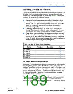
Preliminary, Correlated, and Final Timing
Timing models can have either preliminary, correlated, or final status. The
Quartus II software issues an informational message during design
compilation if the timing models are preliminary. Table 4–43 shows the
status of the Arria GX device timing models.
■
Preliminary status means the timing model is subject to change.
Initially, timing numbers are created using simulation results,
process data, and other known parameters. These tests are used to
make the preliminary numbers as close to the actual timing
parameters as possible.
■
■
Correlated numbers are based on actual device operation and
testing. These numbers reflect the actual performance of the device
under worst-case voltage and junction temperature conditions.
Final timing numbers are based on complete correlation to actual
devices and addressing any minor deviations from the correlated
timing model. When the timing models are final, all or most of the
Arria GX family devices have been completely characterized and no
further changes to the timing model are expected.
Table 4–43. Arria GX Device Timing Model Status
Device
Preliminary
Correlated
Final
EP1AGX20
v
v
v
v
v
EP1AGX35
EP1AGX50
EP1AGX60
EP1AGX90
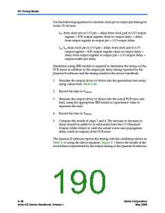
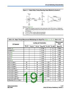
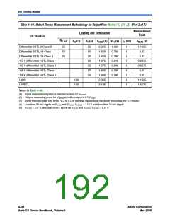
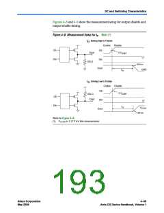
I/O Timing Measurement Methodology
Different I/O standards require different baseline loading techniques for
reporting timing delays. Altera characterizes timing delays with the
required termination for each I/O standard and with 0 pF (except for PCI
and PCI-X which use 10 pF) loading and the timing is specified up to the
output pin of the FPGA device. The Quartus II software calculates the
I/O timing for each I/O standard with a default baseline loading as
specified by the I/O standards.
The following measurements are made during device characterization.
Altera measures clock-to-output delays (tCO) at worst-case process,
minimum voltage, and maximum temperature (PVT) for default loading
conditions shown in Table 4–44.
Altera Corporation
May 2008
4–35
Arria GX Device Handbook, Volume 1

 ALTERA [ ALTERA CORPORATION ]