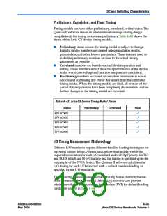
I/O Timing Model
Use the following equations to calculate clock pin to output pin timing for
Arria GX devices:
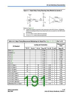
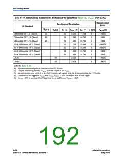
tCO from clock pin to I/O pin = delay from clock pad to I/O output
register + IOE output register clock-to-output delay + delay
from output register to output pin + I/O output delay
txz/tzx from clock pin to I/O pin = delay from clock pad to I/O
output register + IOE output register clock-to-output delay +
delay from output register to output pin + I/O output delay +
output enable pin delay
Simulation using IBIS models is required to determine the delays on the
PCB traces in addition to the output pin delay timing reported by the
Quartus II software and the timing model in the device handbook.
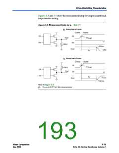
1. Simulate the output driver of choice into the generalized test setup,
using values from Table 4–44.
2. Record the time to VMEAS
.
3. Simulate the output driver of choice into the actual PCB trace and
load, using the appropriate IBIS model or capacitance value to
represent the load.
4. Record the time to VMEAS
.
5. Compare the results of steps 2 and 4. The increase or decrease in
delay should be added to or subtracted from the I/O Standard
Output Adder delays to yield the actual worst-case propagation
delay (clock-to-output) of the PCB trace.
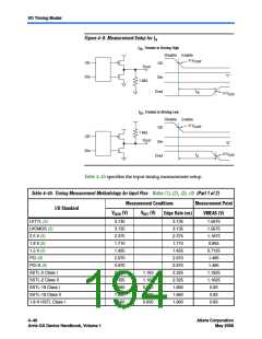
The Quartus II software reports the timing with the conditions shown in
Table 4–44 using the above equation. Figure 4–7 shows the model of the
circuit that is represented by the output timing of the Quartus II software.
4–36
Arria GX Device Handbook, Volume 1
Altera Corporation
May 2008

 ALTERA [ ALTERA CORPORATION ]