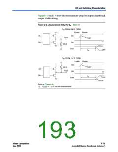
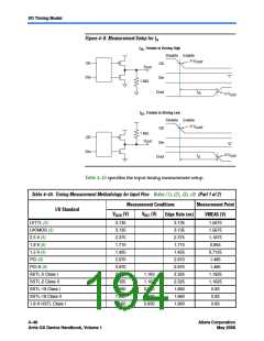
DC and Switching Characteristics
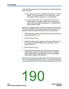
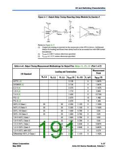
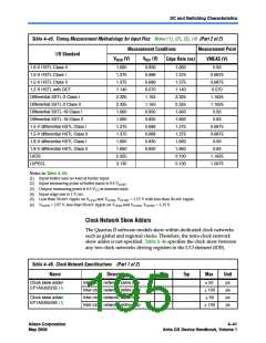
Figure 4–7. Output Delay Timing Reporting Setup Modeled by Quartus II
V
TT
V
CCIO
Output
Output
R
C
p
n
T
L
R
S
Output
Output
Buffer
R
D
V
MEAS
GND
GND
Notes to Figure 4–7:
(1) Output pin timing is reported at the output pin of the FPGA device. Additional
delays for loading and board trace delay need to be accounted for with IBIS model
simulations.
(2) VCCPD is 3.085 V unless otherwise specified.
(3) VCCINT is 1.12 V unless otherwise specified.
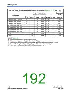
Table 4–44. Output Timing Measurement Methodology for Output Pins Notes (1), (2), (3) (Part 1 of 2)
Measurement
Loading and Termination
Point
I/O Standard
RS (Ω)
RD (Ω)
RT (Ω) VCCIO (V) VTT (V) CL (pF)
VMEAS (V)
LVTTL (4)
3.135
3.135
2.375
1.710
1.425
2.970
2.970
2.325
2.325
1.660
1.660
1.660
1.660
1.375
1.375
1.140
2.325
0
0
1.5675
1.5675
1.1875
0.855
0.7125
1.485
1.485
1.1625
1.1625
0.83
LVCMOS (4)
2.5 V (4)
0
1.8 V (4)
0
1.5 V (4)
0
PCI (5)
10
10
0
PCI-X (5)
SSTL-2 Class I
SSTL-2 Class II
SSTL-18 Class I
SSTL-18 Class II
1.8-V HSTL Class I
1.8-V HSTL Class II
1.5-V HSTL Class I
1.5-V HSTL Class II
1.2-V HSTL with OCT
Differential SSTL-2 Class I
25
25
25
25
50
25
50
25
50
25
50
25
1.123
1.123
0.790
0.790
0.790
0.790
0.648
0.648
0
0
0
0.83
0
0.83
0
0.83
0
0.6875
0.6875
0.570
1.1625
0
0
25
50
1.123
0
Altera Corporation
May 2008
4–37
Arria GX Device Handbook, Volume 1

 ALTERA [ ALTERA CORPORATION ]