DC and Switching Characteristics
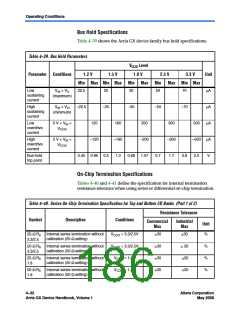
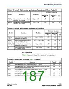
Table 4–40. Series On-Chip Termination Specification for Top and Bottom I/O Banks (Part 2 of 2)
Resistance Tolerance
Symbol
Description
Conditions
Commercial
Industrial
Max
Unit
Max
50-Ω RS
1.5
Internal series termination without
calibration (50-Ω setting)
VCCIO = 1.5V
VCCIO = 1.2V
36
36
%
50-Ω RS
Internal series termination without
50
50
%
calibration (50-Ω setting)
1.2
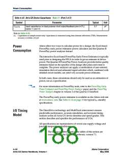
Table 4–41. Series On-Chip Termination Specification for Left I/O Banks
Resistance Tolerance
Commercial Industrial
Symbol
Description
Conditions
Unit
Max
Max
25-Ω RS
3.3/2.5
Internal series termination without
calibration (25-Ω setting)
VCCIO = 3.3/2.5V
VCCIO = 3.3/2.5/1.8V
VCCIO = 1.5V
30
30
%
50-Ω RS
3.3/2.5/1.8
Internal series termination without
calibration (50-Ω setting)
30
36
20
30
36
25
%
%
%
50-Ω RS 1.5 Internal series termination without
calibration (50-Ω setting)
RD
Internal differential termination for
VCCIO = 3.3 V
LVDS (100-Ω setting)
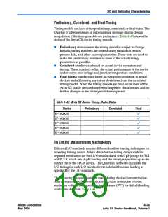
Pin Capacitance
Table 4–42 shows the Arria GX device family pin capacitance.
Table 4–42. Arria GX Device Capacitance Note (1) (Part 1 of 2)
Symbol
Parameter
Typical
5.0
Unit
pF
CIOTB
Input capacitance on I/O pins in I/O banks 3, 4, 7, and 8.
CIOL
Input capacitance on I/O pins in I/O banks 1 and 2, including high-speed
differential receiver and transmitter pins.
6.1
pF
CCLKTB
6.0
pF
Input capacitance on top/bottom clock input pins: CLK[4..7]and
CLK[12..15].
CCLKL
6.1
3.3
pF
pF
Input capacitance on left clock inputs: CLK0and CLK2.
Input capacitance on left clock inputs: CLK1and CLK3.
CCLKL+
Altera Corporation
May 2008
4–33
Arria GX Device Handbook, Volume 1

 ALTERA [ ALTERA CORPORATION ]