Design Considerations
■
Consider a case where eight bidirectional pads are controlled by
OE1, eight bidirectional pads are controlled by OE2, six bidirectional
pads are controlled by OE3, and there are no other outputs or
voltage-referenced inputs in the bank. While this totals 22
bidirectional pads, it is safely allowable because there would be a
possible maximum of 16 outputs per VREF pin, assuming the worst
case where OE1 and OE2 are active and OE3 is inactive. This is useful
for DDR SDRAM applications.
■
When at least one additional voltage-referenced input and no other
outputs exist in the same VREF group, the bidirectional pad limitation
must simultaneously adhere to the input and output limitations. The
input rule becomes:
<Total number of bidirectional pins> + <Total number of VREF input pins>
40 per VREF pin
Whereas the output rule is simplified as:
<Total number of bidirectional pins> 20 per VREF pin
■
■
When at least one additional output exists but no voltage-referenced
inputs exist, the output rule becomes:
<Total number of bidirectional pins> + <Total number of output pins> –
<Total number of pins from smallest OE group> 20 per VREF pin
When additional voltage-referenced inputs and other outputs exist
in the same VREF group, then the bidirectional pad limitation must
again simultaneously adhere to the input and output limitations. The
input rule is:
<Total number of bidirectional pins> + <Total number of VREF input pins>
40 per VREF pin
Whereas the output rule is given as:
<Total number of bidirectional pins> + <Total number of output pins> –
<Total number of pins from smallest OE group> 20 per VREF pin
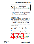
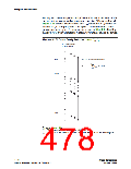
I/O Pin Placement with Respect to High-Speed Differential I/O Pins
Regardless of whether or not the SERDES circuitry is utilized, there is a
restriction on the placement of single-ended output pins with respect to
high-speed differential I/O pins. As shown in Figure 4–25, all
4–38
Stratix II Device Handbook, Volume 2
Altera Corporation
January 2008

 ALTERA [ ALTERA CORPORATION ]