Selectable I/O Standards in Stratix II and Stratix II GX Devices
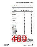
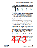
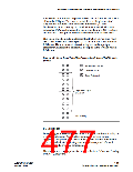
Table 4–8. Acceptable Input Levels for LVTTL and LVCMOS (Part 2 of 2)
Acceptable Input Levels (V)
Bank VCCIO
(V)
3.3
2.5
1.8
v
v
1.5
v (1)
v
1.8
1.5
v (2)
v (2)
v (2)
v (2)
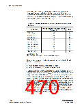
Notes to Table 4–8:
(1) Because the input signal does not drive to the rail, the input buffer does not
completely shut off, and the I/O current is slightly higher than the default value.
(2) These input values overdrive the input buffer, so the pin leakage current is
slightly higher than the default value. To drive inputs higher than VCCIO but less
than 4.0 V, disable the PCI clamping diode and select the Allow LVTTL and
LVCMOS input levels to overdrive input buffer option in the Quartus II
software.
Voltage-Referenced Standards
To accommodate voltage-referenced I/O standards, each Stratix II or
Stratix II GX device’s I/O bank supports multiple VREF pins feeding a
common VREF bus. The number of available VREF pins increases as device
density increases. If these pins are not used as VREF pins, they cannot be
used as generic I/O pins. However, each bank can only have a single
VCCIO voltage level and a single VREF voltage level at a given time.
An I/O bank featuring single-ended or differential standards can support
voltage-referenced standards as long as all voltage-referenced standards
use the same VREF setting.
Because of performance reasons, voltage-referenced input standards use
their own VCCIO level as the power source. For example, you can only
place 1.5-V HSTL input pins in an I/O bank with a 1.5-V VCCIO
.
1
Refer to the “Stratix II and Stratix II GX I/O Banks” on
page 4–20 for details on input VCCIO for voltage-referenced
standards.
Voltage-referenced bidirectional and output signals must be the same as
the I/O bank’s VCCIO voltage. For example, you can only place SSTL-2
output pins in an I/O bank with a 2.5-V VCCIO
.
1
Refer to the “I/O Placement Guidelines” on page 4–36 for
details on voltage-referenced I/O standards placement.
Altera Corporation
January 2008
4–35
Stratix II Device Handbook, Volume 2

 ALTERA [ ALTERA CORPORATION ]