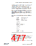
Design Considerations
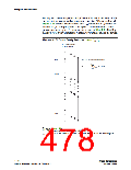
For any ten consecutive pads in an I/O bank of Stratix II and Stratix II GX
devices, Altera recommends a maximum current of 250 mA, as shown in
Figure 4–26, because the placement of VCCIO/ground (GND) bumps are
regular, 10 I/O pins per pair of power pins. This limit is on the static
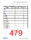
power consumed by an I/O standard, as shown in Table 4–10. Limiting
static power is a way to improve reliability over the lifetime of the device.
Figure 4–26. DC Current Density Restriction Notes (1), (2)
I/O Pin Sequence
of an I/O Bank
VCC
GND
Any 10 Consecutive Output Pins
pin+9
≤
250mA
I
∑
pin
pin
VCC
Notes to Figure 4–26:
(1) The consecutive pads do not cross I/O banks.
(2) VREF pins do not affect DC current calculation because there are no VREF pads.
4–40
Stratix II Device Handbook, Volume 2
Altera Corporation
January 2008

 ALTERA [ ALTERA CORPORATION ]