Design Considerations
Mixing Voltage-Referenced and Non-Voltage-Referenced Standards
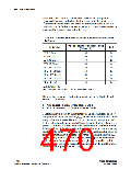
An I/O bank can support both non-voltage-referenced and
voltage-referenced pins by applying each of the rule sets individually. For
example, an I/O bank can support SSTL-18 inputs and 1.8-V inputs and
outputs with a 1.8-V VCCIO and a 0.9-V VREF. Similarly, an I/O bank can
support 1.5-V standards, 2.5-V (inputs, but not outputs), and HSTL I/O
standards with a 1.5-V VCCIO and 0.75-V VREF
.
I/O Placement Guidelines
The I/O placement guidelines help to reduce noise issues that may be
associated with a design such that Stratix II and Stratix II GX FPGAs can
maintain an acceptable noise level on the VCCIO supply. Because Stratix II
and Stratix II GX devices require each bank to be powered separately for
VCCIO, these noise issues have no effect when crossing bank boundaries
and, as such, these rules need not be applied.
This section provides I/O placement guidelines for the programmable
I/O standards supported by Stratix II and Stratix II GX devices and
includes essential information for designing systems using their devices’
selectable I/O capabilities.
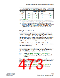
VREF Pin Placement Restrictions
There are at least two dedicated VREF pins per I/O bank to drive the VREF
bus. Larger Stratix II and Stratix II GX devices have more VREF pins per
I/O bank. All VREF pins within one I/O bank are shorted together at
device die level.
There are limits to the number of pins that a VREF pin can support. For
example, each output pin adds some noise to the VREF level and an
excessive number of outputs make the level too unstable to be used for
incoming signals.
Restrictions on the placement of single-ended voltage-referenced I/O
pads with respect to VREF pins help maintain an acceptable noise level on
the VCCIO supply and prevent output switching noise from shifting the
VREF rail.
Input Pins
Each VREF pin supports a maximum of 40 input pads.
4–36
Stratix II Device Handbook, Volume 2
Altera Corporation
January 2008

 ALTERA [ ALTERA CORPORATION ]